Custom Search
|
|
  |
|
|
Figure 3-9A. - Tunnel diode energy diagram with 600 millivolts bias.
Figure 3-9B. - Tunnel diode energy diagram with 600 millivolts bias.
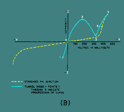
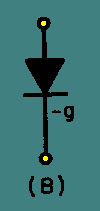
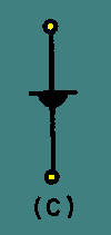
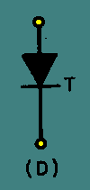
The negative resistance region is the most important and most widely used characteristic of the tunnel diode. A tunnel diode biased to operate in the negative resistance region can be used as either an oscillator or an amplifier in a wide range of frequencies and applications. Very high frequency applications using the tunnel diode are possible because the tunneling action occurs so rapidly that there is no transit time effect and therefore no signal distortion. Tunnel diodes are also used extensively in high-speed switching circuits because of the speed of the tunneling action. Several schematic symbols are used to indicate a tunnel diode. These symbols are illustrated in figure 3-10 (view A, view B, view C, and view D). Figure 3-10A. - Tunnel diode schematic symbols.
Figure 3-10B. - Tunnel diode schematic symbols.
Figure 3-10C. - Tunnel diode schematic symbols.
Figure 3-10D. - Tunnel diode schematic symbols.
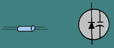
Varactor The VARACTOR, or varicap, as the schematic drawing in figure 3-11 suggests, is a diode that behaves like a variable capacitor, with the PN junction functioning like the dielectric and plates of a common capacitor. Understanding how the varactor operates is an important prerequisite to understanding field-effect transistors, which will be covered later in this topic. Figure 3-11. - Varactor diode.
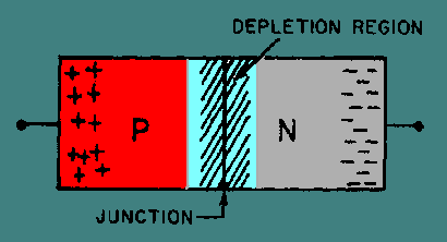
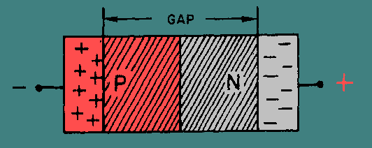
Figure 3-12 shows a PN junction. Surrounding the junction of the P and N materials is a narrow region void of both positively and negatively charged current carriers. This area is called the depletion region. Figure 3-12. - PN junction.
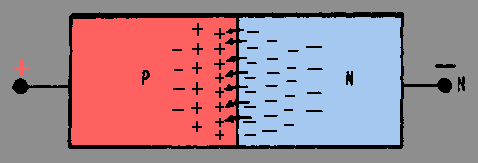
The size of the depletion region in a varactor diode is directly related to the bias. Forward biasing makes the region smaller by repelling the current carriers toward the PN junction. If the applied voltage is large enough (about .5 volt for silicon material), the negative particles will cross the junction and join with the positive particles, as shown in figure 3-13. This forward biasing causes the depletion region to decrease, producing a low resistance at the PN junction and a large current flow across it. This is the condition for a forward-biased diode. On the other hand, if reverse-bias voltage is applied to the PN junction, the size of its depletion region increases as the charged particles on both sides move away from the junction. This condition, shown in figure 3-14, produces a high resistance between the terminals and allows little current flow (only in the microampere range). This is the operating condition for the varactor diode, which is nothing more than a special PN junction. Figure 3-13. - Forward-biased PN junction.
Figure 3-14. - Reverse-biased PN junction.
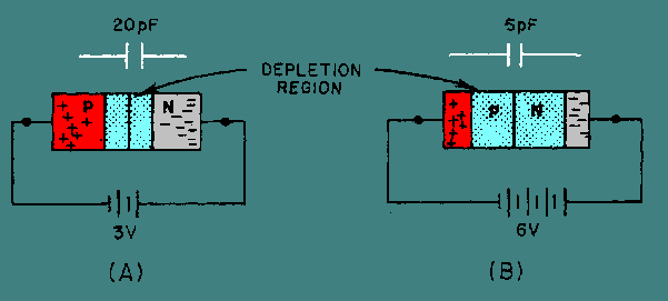
As the figure shows, the insulation gap formed by reverse biasing of the varactor is comparable to the layer of dielectric material between the plates of a common capacitor. Furthermore, the formula used to calculate capacitance
Where A = plate area can be applied to both the varactor and the capacitor. In this case, the size of the insulation gap of the varactor, or depletion region, is substituted for the distance between the plates of the capacitor. By varying the reverse-bias voltage applied to the varactor, the width of the "gap" may be varied. An increase in reverse bias increases the width of the gap (d) which reduces the capacitance (C) of the PN junction. Therefore, the capacitance of the varactor is inversely proportional to the applied reverse bias. The ratio of varactor capacitance to reverse-bias voltage change may be as high as 10 to 1. Figure 3-15 shows one example of the voltage-to-capacitance ratio. View A shows that a reverse bias of 3 volts produces a capacitance of 20 picofarads in the varactor. If the reverse bias is increased to 6 volts, as shown in view B, the depletion region widens and capacitance drops to 5 picofarads. Each 1-volt increase in bias voltage causes a 5-picofarad decrease in the capacitance of the varactor; the ratio of change is therefore 5 to 1. Of course any decrease in applied bias voltage would cause a proportionate increase in capacitance, as the depletion region narrows. Notice that the value of the capacitance is small in the picofarad range. Figure 3-15. - Varactor capacitance versus bias voltage.
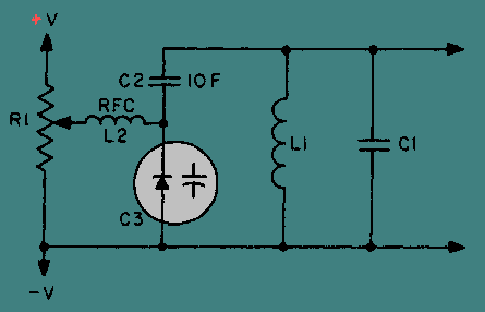
In general, varactors are used to replace the old style variable capacitor tuning. They are used in tuning circuits of more sophisticated communication equipment and in other circuits where variable capacitance is required. One advantage of the varactor is that it allows a dc voltage to be used to tune a circuit for simple remote control or automatic tuning functions. One such application of the varactor is as a variable tuning capacitor in a receiver or transmitter tank circuit like that shown in figure 3-16. Figure 3-16. - Varactor tuned resonant circuit.
Figure 3-16 shows a dc voltage felt at the wiper of potentiometer R1 which can be adjusted between +V and -V. The dc voltage, passed through the low resistance of radio frequency choke L2, acts to reverse bias varactor diode C3. The capacitance of C3 is in series with C2, and the equivalent capacitance of C2 and C3 is in parallel with tank circuit L1-C1. Therefore, any variation in the dc voltage at R1 will vary both the capacitance of C3 and the resonant frequency of the tank circuit. The radio-frequency choke provides high inductive reactance at the tank frequency to prevent tank loading by R1. C2 acts to block dc from the tank as well as to fix the tuning range of C3. An ohmmeter can be used to check a varactor diode in a circuit. A high reverse-bias resistance and a low forward-bias resistance with a 10 to 1 ratio in reverse-bias to forward-bias resistance is considered normal. Q.7 What is the main difference in construction between normal PN junction diodes and
tunnel diodes? |
 |
|
|
Integrated Publishing, Inc. - A (SDVOSB) Service Disabled Veteran Owned Small Business
|