Custom Search
|
|
  |
|
|
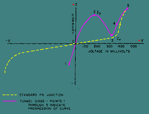
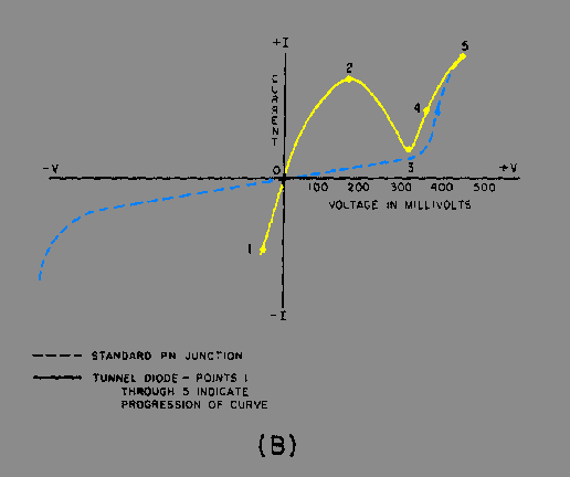
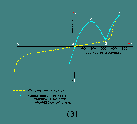
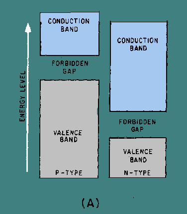
The Tunnel Diode In 1958, Leo Esaki, a Japanese scientist, discovered that if a semiconductor junction diode is heavily doped with impurities, it will have a region of negative resistance. The normal junction diode uses semiconductor materials that are lightly doped with one impurity atom for ten-million semiconductor atoms. This low doping level results in a relatively wide depletion region. Conduction occurs in the normal junction diode only if the voltage applied to it is large enough to overcome the potential barrier of the junction. In the TUNNEL DIODE, the semiconductor materials used in forming a junction are doped to the extent of one-thousand impurity atoms for ten-million semiconductor atoms. This heavy doping produces an extremely narrow depletion zone similar to that in the Zener diode. Also because of the heavy doping, a tunnel diode exhibits an unusual current-voltage characteristic curve as compared with that of an ordinary junction diode. The characteristic curve for a tunnel diode is illustrated in figure 3-5. Figure 3-5. - Characteristic curve of a tunnel diode compared to that of a standard PN junction.
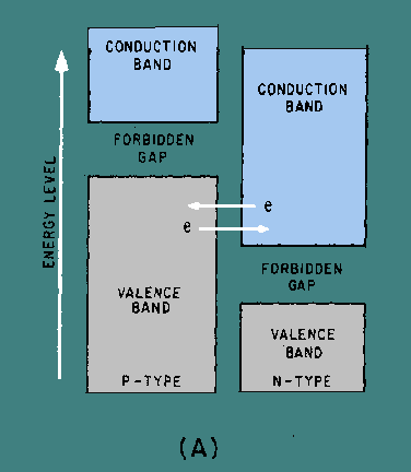
The three most important aspects of this characteristic curve are (1) the forward current increase to a peak (IP) with a small applied forward bias, (2) the decreasing forward current with an increasing forward bias to a minimum valley current (IV), and (3) the normal increasing forward current with further increases in the bias voltage. The portion of the characteristic curve between IP and IV is the region of negative resistance. An explanation of why a tunnel diode has a region of negative resistance is best understood by using energy levels as in the previous explanation of the Zener effect. Simply stated the theory known as quantum-mechanical tunneling is an electron crossing a PN-junction without having sufficient energy to do so otherwise. Because of the heavy doping the width of the depletion region is only one-millionth of an inch. You might think of the process simply as an arc-over between the N- and the P-side across the depletion region. Figure 3-6 shows the equilibrium energy level diagram of a tunnel diode with no bias applied. Note in view A that the valence band of the P-material overlaps the conduction band of the N-material. The majority electrons and holes are at the same energy level in the equilibrium state. If there is any movement of current carriers across the depletion region due to thermal energy, the net current flow will be zero because equal numbers of current carriers flow in opposite directions. The zero net current flow is marked by a "0" on the current-voltage curve illustrated in view B. Figure 3-6A. - Tunnel diode energy diagram with no bias.
Figure 3-6B. - Tunnel diode energy diagram with no bias.
Figure 3-7, view A, shows the energy diagram of a tunnel diode with a small forward bias (50 millivolts) applied. The bias causes unequal energy levels between some of the majority carriers at the energy band overlap point, but not enough of a potential difference to cause the carriers to cross the forbidden gap in the normal manner. Since the valence band of the P-material and the conduction band of the N-material still overlap, current carriers tunnel across at the overlap and cause a substantial current flow. The amount of current flow is marked by point 2 on the curve in view B. Note in view A that the amount of overlap between the valence band and the conduction band decreased when forward bias was applied. Figure 3-7A. - Tunnel diode energy diagram with 50 millivolts bias.
Figure 3-7B. - Tunnel diode energy diagram with 50 millivolts bias.
Figure 3-8, view A, is the energy diagram of a tunnel diode in which the forward bias has been increased to 450 millivolts. As you can see, the valence band and the conduction band no longer overlap at this point, and tunneling can no longer occur. The portion of the curve in view B from point 2 to point 3 shows the decreasing current that occurs as the bias is increased, and the area of overlap becomes smaller. As the overlap between the two energy bands becomes smaller, fewer and fewer electrons can tunnel across the junction. The portion of the curve between point 2 and point 3 in which current decreases as the voltage increases is the negative resistance region of the tunnel diode. Figure 3-8A. - Tunnel diode energy diagram with 450 millivolts bias.
Figure 3-8B. - Tunnel diode energy diagram with 450 millivolts bias.
Figure 3-9, view A, is the energy diagram of a tunnel diode in which the forward bias has been increased even further. The energy bands no longer overlap and the diode operates in the same manner as a normal PN junction, as shown by the portion of the curve in view (B) from point 3 to point 4. |
 |
|
|
Integrated Publishing, Inc. - A (SDVOSB) Service Disabled Veteran Owned Small Business
|