Custom Search
|
|
  |
|
|
LEARNING OBJECTIVES Upon completion of this chapter, you will be able to:
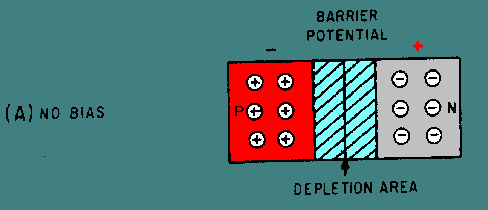
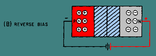
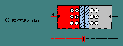
INTRODUCTION TO SPECIAL DEVICES If you consider the sensitive nature and the various interacting properties of semiconductors, it should not be surprising to you that solid state devices can be designed for many different purposes. In fact, devices with special features are so numerous and new designs are so frequently introduced that it would be beyond the scope of this chapter to describe all of the devices in use today. Therefore, this chapter will include a variety of representative devices that are used extensively in Navy equipment to give you an idea of the diversity and versatility that have been made possible. These devices have been grouped into three categories: diodes, optoelectronic devices, and transistors. In this chapter each device will be described and the basic operation of each one will be discussed. DIODES Diodes are two terminal semiconductors of various types that are used in seemingly endless applications. The operation of normal PN-junction diodes has already been discussed, but there are a number of diodes with special properties with which you should be familiar. A discussion of all of the developments in the diode field would be impossible so some of the more commonly used special diodes have been selected for explanation. These include Zener diodes, tunnel diodes, varactors, silicon controlled rectifiers (SCR), and TRIACs. Zener Diodes When a PN-junction diode is reverse biased, the majority carriers (holes in the P-material and electrons in the N-material) move away from the junction. The barrier or depletion region becomes wider, as illustrated in figure 3-1, (view A, view B, view C) and majority carrier current flow becomes very difficult across the high resistance of the wide depletion region. The presence of minority carriers causes a small leakage current that remains nearly constant for all reverse voltages up to a certain value. Once this value has been exceeded, there is a sudden increase in the reverse current. The voltage at which the sudden increase in current occurs is called the BREAKDOWN VOLTAGE. At breakdown, the reverse current increases very rapidly with a slight increase in the reverse voltage. Any diode can be reverse biased to the point of breakdown, but not every diode can safely dissipate the power associated with breakdown. A Zener diode is a PN junction designed to operate in the reverse-bias breakdown region. Figure 3-1A. - Effects of bias on the depletion region of a PN junction.
Figure 3-1B. - Effects of bias on the depletion region of a PN junction.
Figure 3-1C. - Effects of bias on the depletion region of a PN junction.
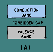
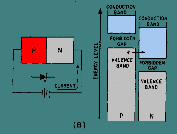
There are two distinct theories used to explain the behavior of PN junctions during breakdown: one is the ZENER EFFECT and the other is the AVALANCHE EFFECT. The ZENER EFFECT was first proposed by Dr. Carl Zener in 1934. According to Dr. Zener's theory, electrical breakdown in solid dielectrics occurs by a process called QUANTUM-MECHANICAL TUNNELING. The Zener effect accounts for the breakdown below 5 volts; whereas, above 5 volts the breakdown is caused by the avalanche effect. Although the avalanche effect is now accepted as an explanation of diode breakdown, the term Zener diode is used to cover both types. The true Zener effect in semiconductors can be described in terms of energy bands; however, only the two upper energy bands are of interest. The two upper bands, illustrated in figure 3-2, view A, are called the conduction band and the valence band. Figure 3-2A. - Energy diagram for Zener diode.
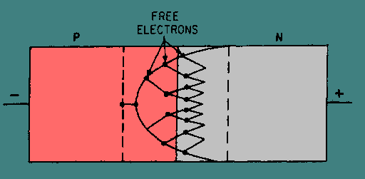
The CONDUCTION BAND is a band in which the energy level of the electrons is high enough that the electrons will move easily under the influence of an external field. Since current flow is the movement of electrons, the readily mobile electrons in the conduction band are capable of maintaining a current flow when an external field in the form of a voltage is applied. Therefore, solid materials that have many electrons in the conduction band are called conductors. The VALENCE BAND is a band in which the energy level is the same as the valence electrons of the atoms. Since the electrons in these levels are attached to the atoms, the electrons are not free to move around as are the conduction band electrons. With the proper amount of energy added, however, the electrons in the valence band may be elevated to the conduction band energy level. To do this, the electrons must cross a gap that exists between the valence band energy level and the conduction band energy level. This gap is known as the FORBIDDEN ENERGY BAND or FORBIDDEN GAP. The energy difference across this gap determines whether a solid material will act as a conductor, a semiconductor, or an insulator. A conductor is a material in which the forbidden gap is so narrow that it can be considered nonexistent. A semiconductor is a solid that contains a forbidden gap, as shown in figure 3-2, view A. Normally, a semiconductor has no electrons at the conduction band energy level. The energy provided by room temperature heat, however, is enough energy to overcome the binding force of a few valence electrons and to elevate them to the conduction band energy level. The addition of impurities to the semiconductor material increases both the number of free electrons in the conduction band and the number of electrons in the valence band that can be elevated to the conduction band. Insulators are materials in which the forbidden gap is so large that practically no electrons can be given enough energy to cross the gap. Therefore, unless extremely large amounts of heat energy are available, these materials will not conduct electricity. View B of figure 3-2 is an energy diagram of a reverse-biased Zener diode. The energy bands of the P and N materials are naturally at different levels, but reverse bias causes the valence band of the P material to overlap the energy level of the conduction band in the N material. Under this condition, the valence electrons of the P material can cross the extremely thin junction region at the overlap point without acquiring any additional energy. This action is called tunneling. When the breakdown point of the PN junction is reached, large numbers of minority carriers "tunnel" across the junction to form the current that occurs at breakdown. The tunneling phenomenon only takes place in heavily doped diodes such as Zener diodes. Figure 3-2B. - Energy diagram for Zener diode.
The second theory of reverse breakdown effect in diodes is known as AVALANCHE breakdown and occurs at reverse voltages beyond 5 volts. This type of breakdown diode has a depletion region that is deliberately made narrower than the depletion region in the normal PN-junction diode, but thicker than that in the Zener-effect diode. The thicker depletion region is achieved by decreasing the doping level from the level used in Zener-effect diodes. The breakdown is at a higher voltage because of the higher resistivity of the material. Controlling the doping level of the material during the manufacturing process can produce breakdown voltages ranging between about 2 and 200 volts. The mechanism of avalanche breakdown is different from that of the Zener effect. In the depletion region of a PN junction, thermal energy is responsible for the formation of electron-hole pairs. The leakage current is caused by the movement of minority electrons, which is accelerated in the electric field across the barrier region. As the reverse voltage across the depletion region is increased, the reverse voltage eventually reaches a critical value. Once the critical or breakdown voltage has been reached, sufficient energy is gained by the thermally released minority electrons to enable the electrons to rupture covalent bonds as they collide with lattice atoms. The released electrons are also accelerated by the electric field, resulting in the release of further electrons, and so on, in a chain or avalanche effect. This process is illustrated in figure 3-3. Figure 3-3. - Avalanche multiplication.
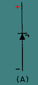
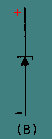
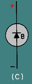
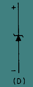
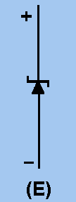
For reverse voltage slightly higher than breakdown, the avalanche effect releases an almost unlimited number of carriers so that the diode essentially becomes a short circuit. The current flow in this region is limited only by an external series current-limiting resistor. Operating a diode in the breakdown region does not damage it, as long as the maximum power dissipation rating of the diode is not exceeded. Removing the reverse voltage permits all carriers to return to their normal energy values and velocities. Some of the symbols used to represent Zener diodes are illustrated in figure 3-4 (view A, view B, view C, view D, and view E). Note that the polarity markings indicate electron flow is with the arrow symbol instead of against it as in a normal PN-junction diode. This is because breakdown diodes are operated in the reverse-bias mode, which means the current flow is by minority current carriers. Figure 3-4A. - Schematic symbols for Zener diodes.
Figure 3-4B. - Schematic symbols for Zener diodes.
Figure 3-4C. - Schematic symbols for Zener diodes.
Figure 3-4D. - Schematic symbols for Zener diodes.
Figure 3-4E. - Schematic symbols for Zener diodes.
Zener diodes of various sorts are used for many purposes, but their most widespread use is as voltage regulators. Once the breakdown voltage of a Zener diode is reached, the voltage across the diode remains almost constant regardless of the supply voltage. Therefore they hold the voltage across the load at a constant level. This characteristic makes Zener diodes ideal voltage regulators, and they are found in almost all solid-state circuits in this capacity. Q.1 In a reverse biased PN-junction, which current carriers cause leakage current? |
 |
|
|
Integrated Publishing, Inc. - A (SDVOSB) Service Disabled Veteran Owned Small Business
|