Custom Search
|
|
  |
|||||||||||||||||||||||||||||
|
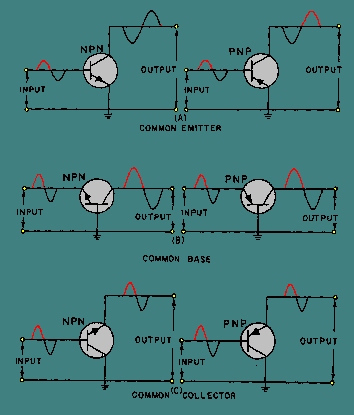
TRANSISTOR CONFIGURATIONS A transistor may be connected in any one of three basic configurations (fig. 2-16): common emitter (CE), common base (CB), and common collector (CC). The term common is used to denote the element that is common to both input and output circuits. Because the common element is often grounded, these configurations are frequently referred to as grounded emitter, grounded base, and grounded collector. Figure 2-16. - Transistor configurations.
Each configuration, as you will see later, has particular characteristics that make it suitable for specific applications. An easy way to identify a specific transistor configuration is to follow three simple steps:
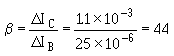
Therefore, by applying these three simple steps to the circuit in figure 2-12, we can conclude that this circuit is more than just a basic transistor amplifier. It is a common-emitter amplifier. Common Emitter The common-emitter configuration (CE) shown in figure 2-16 view A is the arrangement most frequently used in practical amplifier circuits, since it provides good voltage, current, and power gain. The common emitter also has a somewhat low input resistance (500 ohms-1500 ohms), because the input is applied to the forward-biased junction, and a moderately high output resistance (30 kilohms-50 kilohms or more), because the output is taken off the reverse-biased junction. Since the input signal is applied to the base-emitter circuit and the output is taken from the collector-emitter circuit, the emitter is the element common to both input and output. Since you have already covered what you now know to be a common-emitter amplifier (fig. 2-12), let's take a few minutes and review its operation, using the PNP common-emitter configuration shown in figure 2-16 view A. When a transistor is connected in a common-emitter configuration, the input signal is injected between the base and emitter, which is a low resistance, low-current circuit. As the input signal swings positive, it also causes the base to swing positive with respect to the emitter. This action decreases forward bias which reduces collector current (IC) and increases collector voltage (making VC more negative). During the negative alternation of the input signal, the base is driven more negative with respect to the emitter. This increases forward bias and allows more current carriers to be released from the emitter, which results in an increase in collector current and a decrease in collector voltage (making VC less negative or swing in a positive direction). The collector current that flows through the high resistance reverse-biased junction also flows through a high resistance load (not shown), resulting in a high level of amplification. Since the input signal to the common emitter goes positive when the output goes negative, the two signals (input and output) are 180 degrees out of phase. The common-emitter circuit is the only configuration that provides a phase reversal. The common-emitter is the most popular of the three transistor configurations because it has the best combination of current and voltage gain. The term GAIN is used to describe the amplification capabilities of the amplifier. It is basically a ratio of output versus input. Each transistor configuration gives a different value of gain even though the same transistor is used. The transistor configuration used is a matter of design consideration. However, as a technician you will become interested in this output versus input ratio (gain) to determine whether or not the transistor is working properly in the circuit. The current gain in the common-emitter circuit is called BETA (b). Beta is the relationship of collector current (output current) to base current (input current). To calculate beta, use the following formula:
(D is the Greek letter delta, it is used to indicate a small change) For example, if the input current (IB) in a common emitter changes from 75 mA to 100 mA and the output current (IC) changes from 1.5 mA to 2.6 mA, the current gain (b) will be 44.
This simply means that a change in base current produces a change in collector current which is 44 times as large. You may also see the term hfe used in place of b. The terms hfe and b are equivalent and may be used interchangeably. This is because "hfe" means: h = hybrid (meaning mixture)f = forward current transfer ratio The resistance gain of the common emitter can be found in a method similar to the one used for finding beta:
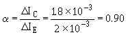
Once the resistance gain is known, the voltage gain is easy to calculate since it is equal to the current gain ( b) multiplied by the resistance gain (E = bR). And, the power gain is equal to the voltage gain multiplied by the current gain b (P = bE).Common Base The common-base configuration (CB) shown in figure 2-16, view B is mainly used for impedance matching, since it has a low input resistance (30 ohms-160 ohms) and a high output resistance (250 kilohms-550 kilohms). However, two factors limit its usefulness in some circuit applications: (1) its low input resistance and (2) its current gain of less than 1. Since the CB configuration will give voltage amplification, there are some additional applications, which require both a low-input resistance and voltage amplification, that could use a circuit configuration of this type; for example, some microphone amplifiers. In the common-base configuration, the input signal is applied to the emitter, the output is taken from the collector, and the base is the element common to both input and output. Since the input is applied to the emitter, it causes the emitter-base junction to react in the same manner as it did in the common-emitter circuit. For example, an input that aids the bias will increase transistor current, and one that opposes the bias will decrease transistor current. Unlike the common-emitter circuit, the input and output signals in the common-base circuit are in phase. To illustrate this point, assume the input to the PNP version of the common-base circuit in figure 2-16 view B is positive. The signal adds to the forward bias, since it is applied to the emitter, causing the collector current to increase. This increase in Ic results in a greater voltage drop across the load resistor RL (not shown), thus lowering the collector voltage VC. The collector voltage, in becoming less negative, is swinging in a positive direction, and is therefore in phase with the incoming positive signal. The current gain in the common-base circuit is calculated in a method similar to that of the common emitter except that the input current is I E not IB and the term ALPHA (a) is used in place of beta for gain. Alpha is the relationship of collector current (output current) to emitter current (input current). Alpha is calculated using the formula:
For example, if the input current (IE) in a common base changes from 1 mA to 3 mA and the output current (IC) changes from 1 mA to 2.8 mA, the current gain (a) will be 0.90 or:
This is a current gain of less than 1. Since part of the emitter current flows into the base and does not appear as collector current, collector current will always be less than the emitter current that causes it. (Remember, IE = IB + IC) Therefore, ALPHA is ALWAYS LESS THAN ONE FOR A COMMON-BASE CONFIGURATION. Another term for " a" is hfb. These terms (and hfb) are equivalent and may be used interchangeably. The meaning for the term hfb is derived in the same manner as the term hfe mentioned earlier, except that the last letter "e" has been replaced with "b" to stand for common- base configuration.Many transistor manuals and data sheets only list transistor current gain characteristics in terms of b or hfe. To find alpha (a) when given beta (b), use the following formula to convert b to a for use with the common-base configuration:
To calculate the other gains (voltage and power) in the common-base configuration when the current gain ( a) is known, follow the procedures described earlier under the common-emitter section.Common Collector The common-collector configuration (CC) shown in figure 2-16 view C is used mostly for impedance matching. It is also used as a current driver, because of its substantial current gain. It is particularly useful in switching circuitry, since it has the ability to pass signals in either direction (bilateral operation). In the common-collector circuit, the input signal is applied to the base, the output is taken from the emitter, and the collector is the element common to both input and output. The common collector is equivalent to our old friend the electron-tube cathode follower. Both have high input and low output resistance. The input resistance for the common collector ranges from 2 kilohms to 500 kilohms, and the output resistance varies from 50 ohms to 1500 ohms. The current gain is higher than that in the common emitter, but it has a lower power gain than either the common base or common emitter. Like the common base, the output signal from the common collector is in phase with the input signal. The common collector is also referred to as an emitter-follower because the output developed on the emitter follows the input signal applied to the base. Transistor action in the common collector is similar to the operation explained for the common base, except that the current gain is not based on the emitter-to-collector current ratio, alpha ( a). Instead, it is based on the emitter-to-base current ratio called GAMMA (g), because the output is taken off the emitter. Since a small change in base current controls a large change in emitter current, it is still possible to obtain high current gain in the common collector. However, since the emitter current gain is offset by the low output resistance, the voltage gain is always less than 1 (unity), exactly as in the electron-tube cathode followerThe common-collector current gain, gamma ( g), is defined as
and is related to collector-to-base current gain, beta ( b), of the common-emitter circuit by the formula:
Since a given transistor may be connected in any of three basic configurations, there is a definite relationship, as pointed out earlier, between alpha ( a), beta (b), and gamma (g). These relationships are listed again for your convenience:
Take, for example, a transistor that is listed on a manufacturer's data sheet as having an alpha of 0.90. We wish to use it in a common emitter configuration. This means we must find beta. The calculations are:
Therefore, a change in base current in this transistor will produce a change in collector current that will be 9 times as large. If we wish to use this same transistor in a common collector, we can find gamma ( g) by:
To summarize the properties of the three transistor configurations, a comparison chart is provided in table 2-1 for your convenience. Table 2-1. - Transistor Configuration Comparison Chart
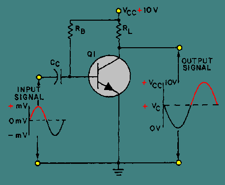
Now that we have analyzed the basic transistor amplifier in terms of bias, class of operation, and circuit configuration, let's apply what has been covered to figure 2-12. A reproduction of figure 2-12 is shown below for your convenience.
This illustration is not just the basic transistor amplifier shown earlier in figure 2-12 but a class A amplifier configured as a common emitter using fixed bias. From this, you should be able to conclude the following:
In conclusion, the type of bias, class of operation, and circuit configuration are all clues to the function and possible application of the amplifier. Q.26 What are the three transistor configurations? |
 |
||||||||||||||||||||||||||||
|
|
Integrated Publishing, Inc. - A (SDVOSB) Service Disabled Veteran Owned Small Business
|