Custom Search
|
|
  |
|
|
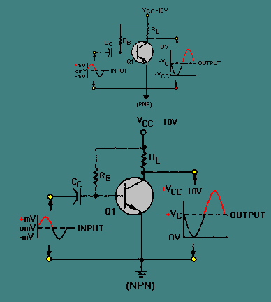
THE BASIC TRANSISTOR AMPLIFIER In the preceding pages we explained the internal workings of the transistor and introduced new terms, such as emitter, base, and collector. Since you should be familiar by now with all of the new terms mentioned earlier and with the internal operation of the transistor, we will move on to the basic transistor amplifier. To understand the overall operation of the transistor amplifier, you must only consider the current in and out of the transistor and through the various components in the circuit. Therefore, from this point on, only the schematic symbol for the transistor will be used in the illustrations, and rather than thinking about majority and minority carriers, we will now start thinking in terms of emitter, base, and collector current. Before going into the basic transistor amplifier, there are two terms you should be familiar with: AMPLIFICATION and AMPLIFIER. Amplification is the process of increasing the strength of a SIGNAL. A signal is just a general term used to refer to any particular current, voltage, or power in a circuit. An amplifier is the device that provides amplification (the increase in current, voltage, or power of a signal) without appreciably altering the original signal. Transistors are frequently used as amplifiers. Some transistor circuits are CURRENT amplifiers, with a small load resistance; other circuits are designed for VOLTAGE amplification and have a high load resistance; others amplify POWER. Now take a look at the NPN version of the basic transistor amplifier in figure 2-12 and let's see just how it works. So far in this discussion, a separate battery has been used to provide the necessary forward-bias voltage. Although a separate battery has been used in the past for convenience, it is not practical to use a battery for emitter-base bias. For instance, it would take a battery slightly over .2 volts to properly forward bias a germanium transistor, while a similar silicon transistor would require a voltage slightly over .6 volts. However, common batteries do not have such voltage values. Also, since bias voltages are quite critical and must be held within a few tenths of one volt, it is easier to work with bias currents flowing through resistors of high ohmic values than with batteries. By inserting one or more resistors in a circuit, different methods of biasing may be achieved and the emitter-base battery eliminated. In addition to eliminating the battery, some of these biasing methods compensate for slight variations in transistor characteristics and changes in transistor conduction resulting from temperature irregularities. Notice in figure 2-12 that the emitter-base battery has been eliminated and the bias resistor RB has been inserted between the collector and the base. Resistor RB provides the necessary forward bias for the emitter-base junction. Current flows in the emitter-base bias circuit from ground to the emitter, out the base lead, and through RB to VCC. Since the current in the base circuit is very small (a few hundred microamperes) and the forward resistance of the transistor is low, only a few tenths of a volt of positive bias will be felt on the base of the transistor. However, this is enough voltage on the base, along with ground on the emitter and the large positive voltage on the collector, to properly bias the transistor. Figure 2-12. - The basic transistor amplifier.
With Q1 properly biased, direct current flows continuously, with or without an input signal, throughout the entire circuit. The direct current flowing through the circuit develops more than just base bias; it also develops the collector voltage (VC) as it flows through Q1 and RL. Notice the collector voltage on the output graph. Since it is present in the circuit without an input signal, the output signal starts at the VC level and either increases or decreases. These dc voltages and currents that exist in the circuit before the application of a signal are known as QUIESCENT voltages and currents (the quiescent state of the circuit). Resistor RL, the collector load resistor, is placed in the circuit to keep the full effect of the collector supply voltage off the collector. This permits the collector voltage (VC) to change with an input signal, which in turn allows the transistor to amplify voltage. Without RL in the circuit, the voltage on the collector would always be equal to VCC. The coupling capacitor (CC) is another new addition to the transistor circuit. It is used to pass the ac input signal and block the dc voltage from the preceding circuit. This prevents dc in the circuitry on the left of the coupling capacitor from affecting the bias on Q1. The coupling capacitor also blocks the bias of Q1 from reaching the input signal source. The input to the amplifier is a sine wave that varies a few millivolts above and below zero. It is introduced into the circuit by the coupling capacitor and is applied between the base and emitter. As the input signal goes positive, the voltage across the emitter-base junction becomes more positive. This in effect increases forward bias, which causes base current to increase at the same rate as that of the input sine wave. Emitter and collector currents also increase but much more than the base current. With an increase in collector current, more voltage is developed across R L. Since the voltage across RL and the voltage across Q1 (collector to emitter) must add up to VCC, an increase in voltage across RL results in an equal decrease in voltage across Q1. Therefore, the output voltage from the amplifier, taken at the collector of Q1 with respect to the emitter, is a negative alternation of voltage that is larger than the input, but has the same sine wave characteristics. During the negative alternation of the input, the input signal opposes the forward bias. This action decreases base current, which results in a decrease in both emitter and collector currents. The decrease in current through RL decreases its voltage drop and causes the voltage across the transistor to rise along with the output voltage. Therefore, the output for the negative alternation of the input is a positive alternation of voltage that is larger than the input but has the same sine wave characteristics. By examining both input and output signals for one complete alternation of the input, we can see that the output of the amplifier is an exact reproduction of the input except for the reversal in polarity and the increased amplitude (a few millivolts as compared to a few volts). The PNP version of this amplifier is shown in the upper part of the figure. The primary difference between the NPN and PNP amplifier is the polarity of the source voltage. With a negative VCC, the PNP base voltage is slightly negative with respect to ground, which provides the necessary forward bias condition between the emitter and base. When the PNP input signal goes positive, it opposes the forward bias of the transistor. This action cancels some of the negative voltage across the emitter-base junction, which reduces the current through the transistor. Therefore, the voltage across the load resistor decreases, and the voltage across the transistor increases. Since VCC is negative, the voltage on the collector (VC) goes in a negative direction (as shown on the output graph) toward -VCC (for example, from -5 volts to -7 volts). Thus, the output is a negative alternation of voltage that varies at the same rate as the sine wave input, but it is opposite in polarity and has a much larger amplitude . During the negative alternation of the input signal, the transistor current increases because the input voltage aids the forward bias. Therefore, the voltage across RL increases, and consequently, the voltage across the transistor decreases or goes in a positive direction (for example: from -5 volts to -3 volts). This action results in a positive output voltage, which has the same characteristics as the input except that it has been amplified and the polarity is reversed. In summary, the input signals in the preceding circuits were amplified because the small change in base current caused a large change in collector current. And, by placing resistor RL in series with the collector, voltage amplification was achieved. Q.14 What is the name of the device that provides an increase in current, voltage, or
power of a signal without appreciably altering the original signal? |
 |