Custom Search
|
|
  |
|
|
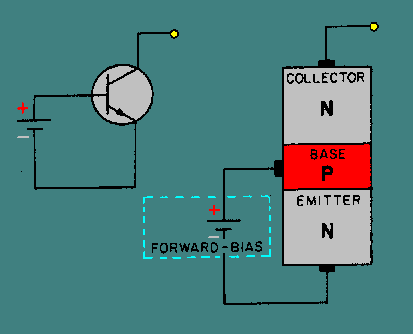
TRANSISTOR THEORY You should recall from an earlier discussion that a forward-biased PN junction is comparable to a low-resistance circuit element because it passes a high current for a given voltage. In turn, a reverse-biased PN junction is comparable to a high-resistance circuit element. By using the Ohm's law formula for power (P = I2R) and assuming current is held constant, you can conclude that the power developed across a high resistance is greater than that developed across a low resistance. Thus, if a crystal were to contain two PN junctions (one forward-biased and the other reverse-biased), a low-power signal could be injected into the forward-biased junction and produce a high-power signal at the reverse-biased junction. In this manner, a power gain would be obtained across the crystal. This concept, which is merely an extension of the material covered in chapter 1, is the basic theory behind how the transistor amplifies. With this information fresh in your mind, let's proceed directly to the NPN transistor. Just as in the case of the PN junction diode, the N material comprising the two end sections of the NP N transistor contains a number of free electrons, while the center P section contains an excess number of holes. The action at each junction between these sections is the same as that previously described for the diode; that is, depletion regions develop and the junction barrier appears. To use the transistor as an amplifier, each of these junctions must be modified by some external bias voltage. For the transistor to function in this capacity, the first PN junction (emitter-base junction) is biased in the forward, or low-resistance, direction. At the same time the second PN junction (base-collector junction) is biased in the reverse, or high-resistance, direction. A simple way to remember how to properly bias a transistor is to observe the NPN or PNP elements that make up the transistor. The letters of these elements indicate what polarity voltage to use for correct bias. For instance, notice the NPN transistor below:
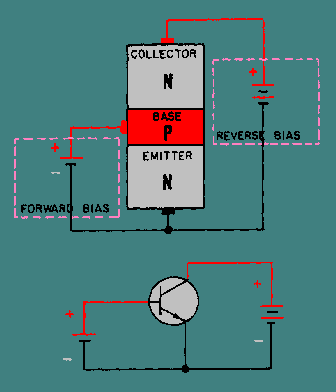
The emitter, which is the first letter in the NPN sequence, is connected to the negative side of the battery while the base, which is the second letter(NPN), is connected to the positive side. However, since the second PN junction is required to be reverse biased for proper transistor operation, the collector must be connected to an opposite polarity voltage(positive) than that indicated by its letter designation(NPN). The voltage on the collector must also be more positive than the base, as shown below:
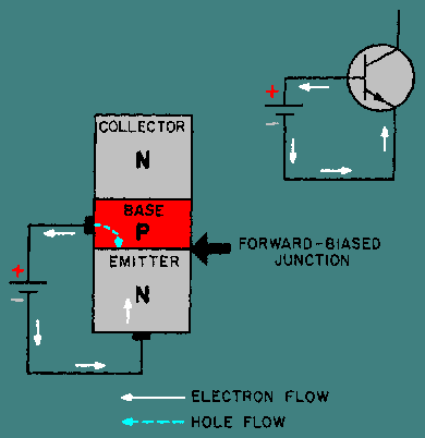
We now have a properly biased NPN transistor. In summary, the base of the NPN transistor must be positive with respect to the emitter, and the collector must be more positive than the base. NPN FORWARD-BIASED JUNCTION. - An important point to bring out at this time, which was not necessarily mentioned during the explanation of the diode, is the fact that the N material on one side of the forward-biased junction is more heavily doped than the P material. This results in more current being carried across the junction by the majority carrier electrons from the N material than the majority carrier holes from the P material. Therefore, conduction through the forward-biased junction, as shown in figure 2-5, is mainly by majority carrier electrons from the N material (emitter). Figure 2-5. - The forward-biased junction in an NPN transistor.
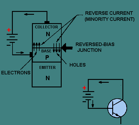
With the emitter-to-base junction in the figure biased in the forward direction, electrons leave the negative terminal of the battery and enter the N material (emitter). Since electrons are majority current carriers in the N material, they pass easily through the emitter, cross over the junction, and combine with holes in the P material (base). For each electron that fills a hole in the P material, another electron will leave the P material (creating a new hole) and enter the positive terminal of the battery. NPN REVERSE-BIASED JUNCTION. - The second PN junction (base-to-collector), or reverse-biased junction as it is called (fig. 2-6), blocks the majority current carriers from crossing the junction. However, there is a very small current, mentioned earlier, that does pass through this junction. This current is called minority current, or reverse current. As you recall, this current was produced by the electron-hole pairs. The minority carriers for the reverse-biased PN junction are the electrons in the P material and the holes in the N material. These minority carriers actually conduct the current for the reverse-biased junction when electrons from the P material enter the N material, and the holes from the N material enter the P material. However, the minority current electrons (as you will see later) play the most important part in the operation of the NPN transistor. Figure 2-6. - The reverse-biased junction in an NPN transistor.
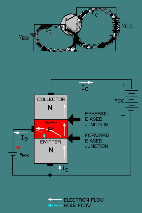
At this point you may wonder why the second PN junction (base-to-collector) is not forward biased like the first PN junction (emitter-to-base). If both junctions were forward biased, the electrons would have a tendency to flow from each end section of the N P N transistor (emitter and collector) to the center P section (base). In essence, we would have two junction diodes possessing a common base, thus eliminating any amplification and defeating the purpose of the transistor. A word of caution is in order at this time. If you should mistakenly bias the second PN junction in the forward direction, the excessive current could develop enough heat to destroy the junctions, making the transistor useless. Therefore, be sure your bias voltage polarities are correct before making any electrical connections. NPN JUNCTION INTERACTION. - We are now ready to see what happens when we place the two junctions of the NPN transistor in operation at the same time. For a better understanding of just how the two junctions work together, refer to figure 2-7 during the discussion. Figure 2-7. - NPN transistor operation.
The bias batteries in this figure have been labeled VCC for the collector voltage supply, and VBB for the base voltage supply. Also notice the base supply battery is quite small, as indicated by the number of cells in the battery, usually 1 volt or less. However, the collector supply is generally much higher than the base supply, normally around 6 volts. As you will see later, this difference in supply voltages is necessary to have current flow from the emitter to the collector. As stated earlier, the current flow in the external circuit is always due to the movement of free electrons. Therefore, electrons flow from the negative terminals of the supply batteries to the N-type emitter. This combined movement of electrons is known as emitter current (IE). Since electrons are the majority carriers in the N material, they will move through the N material emitter to the emitter-base junction. With this junction forward biased, electrons continue on into the base region. Once the electrons are in the base, which is a P-type material, they become minority carriers. Some of the electrons that move into the base recombine with available holes. For each electron that recombines, another electron moves out through the base lead as base current IB (creating a new hole for eventual combination) and returns to the base supply battery V BB . The electrons that recombine are lost as far as the collector is concerned. Therefore, to make the transistor more efficient, the base region is made very thin and lightly doped. This reduces the opportunity for an electron to recombine with a hole and be lost. Thus, most of the electrons that move into the base region come under the influence of the large collector reverse bias. This bias acts as forward bias for the minority carriers (electrons) in the base and, as such, accelerates them through the base-collector junction and on into the collector region. Since the collector is made of an N-type material, the electrons that reach the collector again become majority current carriers. Once in the collector, the electrons move easily through the N material and return to the positive terminal of the collector supply battery VCC as collector current (IC).To further improve on the efficiency of the transistor, the collector is made physically larger than the base for two reasons: (1) to increase the chance of collecting carriers that diffuse to the side as well as directly across the base region, and (2) to enable the collector to handle more heat without damage. In summary, total current flow in the NPN transistor is through the emitter lead. Therefore, in terms of percentage, IE is 100 percent. On the other hand, since the base is very thin and lightly doped, a smaller percentage of the total current (emitter current) will flow in the base circuit than in the collector circuit. Usually no more than 2 to 5 percent of the total current is base current (IB) while the remaining 95 to 98 percent is collector current (IC). A very basic relationship exists between these two currents: IE = IB + IC In simple terms this means that the emitter current is separated into base and collector current. Since the amount of current leaving the emitter is solely a function of the emitter-base bias, and because the collector receives most of this current, a small change in emitter-base bias will have a far greater effect on the magnitude of collector current than it will have on base current. In conclusion, the relatively small emitter-base bias controls the relatively large emitter-to-collector current. Q.6 To properly bias an NPN transistor, what polarity voltage is applied to the
collector, and what is its relationship to the base voltage? |
 |
|
|
Integrated Publishing, Inc. - A (SDVOSB) Service Disabled Veteran Owned Small Business
|