Custom Search
|
|
  |
|
|
TRANSISTORS LEARNING OBJECTIVES Upon completion of this chapter, you should be able to do the following: Define the term transistor and give a brief description of its construction and operation.
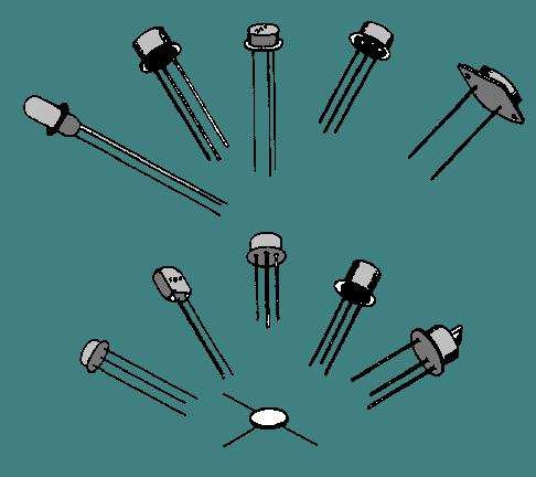
INTRODUCTION TO TRANSISTORS The discovery of the first transistor in 1948 by a team of physicists at the Bell Telephone Laboratories sparked an interest in solid-state research that spread rapidly. The transistor, which began as a simple laboratory oddity, was rapidly developed into a semiconductor device of major importance. The transistor demonstrated for the first time in history that amplification in solids was possible. Before the transistor, amplification was achieved only with electron tubes. Transistors now perform numerous electronic tasks with new and improved transistor designs being continually put on the market. In many cases, transistors are more desirable than tubes because they are small, rugged, require no filament power, and operate at low voltages with comparatively high efficiency. The development of a family of transistors has even made possible the miniaturization of electronic circuits. Figure 2-1 shows a sample of the many different types of transistors you may encounter when working with electronic equipment. Figure 2-1. - An assortment of different types of transistors.
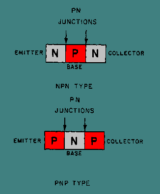
Transistors have infiltrated virtually every area of science and industry, from the family car to satellites. Even the military depends heavily on transistors. The ever increasing uses for transistors have created an urgent need for sound and basic information regarding their operation. From your study of the PN-junction diode in the preceding chapter, you now have the basic knowledge to grasp the principles of transistor operation. In this chapter you will first become acquainted with the basic types of transistors, their construction, and their theory of operation. You will also find out just how and why transistors amplify. Once this basic information is understood, transistor terminology, capabilities, limitations, and identification will be discussed. Last, we will talk about transistor maintenance, integrated circuits, circuit boards, and modular circuitry. The first solid-state device discussed was the two-element semiconductor diode. The next device on our list is even more unique. It not only has one more element than the diode but it can amplify as well. Semiconductor devices that have-three or more elements are called TRANSISTORS. The term transistor was derived from the words TRANSfer and resISTOR. This term was adopted because it best describes the operation of the transistor - the transfer of an input signal current from a low-resistance circuit to a high-resistance circuit. Basically, the transistor is a solid-state device that amplifies by controlling the flow of current carriers through its semiconductor materials. There are many different types of transistors, but their basic theory of operation is all the same. As a matter of fact, the theory we will be using to explain the operation of a transistor is the same theory used earlier with the PN-junction diode except that now two such junctions are required to form the three elements of a transistor. The three elements of the two-junction transistor are (1) the EMITTER, which gives off, or emits," current carriers (electrons or holes); (2) the BASE, which controls the flow of current carriers; and (3) the COLLECTOR, which collects the current carriers. CLASSIFICATION Transistors are classified as either NPN or PNP according to the arrangement of their N and P materials. Their basic construction and chemical treatment is implied by their names, "NPN" or "PNP." That is, an NPN transistor is formed by introducing a thin region of P-type material between two regions of N-type material. On the other hand, a PNP transistor is formed by introducing a thin region of N-type material between two regions of P-type material. Transistors constructed in this manner have two PN junctions, as shown in figure 2-2. One PN junction is between the emitter and the base; the other PN junction is between the collector and the base. The two junctions share one section of semiconductor material so that the transistor actually consists of three elements. Figure 2-2. - Transistor block diagrams.
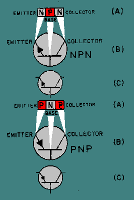
Since the majority and minority current carriers are different for N and P materials, it stands to reason that the internal operation of the NPN and PNP transistors will also be different. The theory of operation of the NPN and PNP transistors will be discussed separately in the next few paragraphs. Any additional information about the PN junction will be given as the theory of transistor operation is developed. To prepare you for the forthcoming information, the two basic types of transistors along with their circuit symbols are shown in figure 2-3. It should be noted that the two symbols are different. The horizontal line represents the base, the angular line with the arrow on it represents the emitter, and the other angular line represents the collector. The direction of the arrow on the emitter distinguishes the NPN from the PNP transistor. If the arrow points in, (Points iN) the transistor is a PNP. On the other hand if the arrow points out, the transistor is an NPN (Not Pointing iN).
Figure 2-3. - Transistor representations.
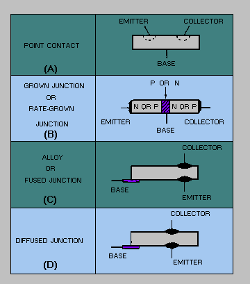
Another point you should keep in mind is that the arrow always points in the direction of hole flow, or from the P to N sections, no matter whether the P section is the emitter or base. On the other hand, electron flow is always toward or against the arrow, just like in the junction diode. CONSTRUCTION The very first transistors were known as point-contact transistors. Their construction is similar to the construction of the point-contact diode covered in chapter 1. The difference, of course, is that the point-contact transistor has two P or N regions formed instead of one. Each of the two regions constitutes an electrode (element) of the transistor. One is named the emitter and the other is named the collector, as shown in figure 2-4, view A. Figure 2-4. - Transistor constructions.
Point-contact transistors are now practically obsolete. They have been replaced by junction transistors, which are superior to point-contact transistors in nearly all respects. The junction transistor generates less noise, handles more power, provides higher current and voltage gains, and can be mass-produced more cheaply than the point-contact transistor. Junction transistors are manufactured in much the same manner as the PN junction diode discussed earlier. However, when the PNP or NPN material is grown (view B), the impurity mixing process must be reversed twice to obtain the two junctions required in a transistor. Likewise, when the alloy-junction (view C) or the diffused-junction (view D) process is used, two junctions must also be created within the crystal. Although there are numerous ways to manufacture transistors, one of the most important parts of any manufacturing process is quality control. Without good quality control, many transistors would prove unreliable because the construction and processing of a transistor govern its thermal ratings, stability, and electrical characteristics. Even though there are many variations in the transistor manufacturing processes, certain structural techniques, which yield good reliability and long life , are common to all processes: (1) Wire leads are connected to each semiconductor electrode; (2) the crystal is specially mounted to protect it against mechanical damage; and (3) the unit is sealed to prevent harmful contamination of the crystal. Q.1 What is the name given to the semiconductor device that has three or more elements?
|
 |