Custom Search
|
|
  |
|
|
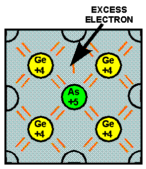
The pure semiconductor mentioned earlier is basically neutral. It contains no free electrons in its conduction bands. Even with the application of thermal energy, only a few covalent bonds are broken, yielding a relatively small current flow. A much more efficient method of increasing current flow in semiconductors is by adding very small amounts of selected additives to them, generally no more than a few parts per million. These additives are called impurities and the process of adding them to crystals is referred to as DOPING. The purpose of semiconductor doping is to increase the number of free charges that can be moved by an external applied voltage. When an impurity increases the number of free electrons, the doped semiconductor is NEGATIVE or N TYPE, and the impurity that is added is known as an N-type impurity. However, an impurity that reduces the number of free electrons, causing more holes, creates a POSITIVE or P-TYPE semiconductor, and the impurity that was added to it is known as a P-type impurity. Semiconductors which are doped in this manner - either with N- or P-type impurities - are referred to as EXTRINSIC semiconductors. N-Type Semiconductor The N-type impurity loses its extra valence electron easily when added to a semiconductor material, and in so doing, increases the conductivity of the material by contributing a free electron. This type of impurity has 5 valence electrons and is called a PENTAVALENT impurity. Arsenic, antimony, bismuth, and phosphorous are pentavalent impurities. Because these materials give or donate one electron to the doped material, they are also called DONOR impurities. When a pentavalent (donor) impurity, like arsenic, is added to germanium, it will form covalent bonds with the germanium atoms. Figure 1-10 illustrates this by showing an arsenic atom (AS) in a germanium (GE) lattice structure. Notice the arsenic atom in the center of the lattice. It has 5 valence electrons in its outer shell but uses only 4 of them to form covalent bonds with the germanium atoms, leaving 1 electron relatively free in the crystal structure. Pure germanium may be converted into an N-type semiconductor by "doping" it with any donor impurity having 5 valence electrons in its outer shell. Since this type of semiconductor (N-type) has a surplus of electrons, the electrons are considered MAJORITY carriers, while the holes, being few in number, are the MINORITY carriers. Figure 1-10. - Germanium crystal doped with arsenic.
P-Type Semiconductor The second type of impurity, when added to a semiconductor material, tends to compensate for its deficiency of 1 valence electron by acquiring an electron from its neighbor. Impurities of this type have only 3 valence electrons and are called TRIVALENT impurities. Aluminum, indium, gallium, and boron are trivalent impurities. Because these materials accept 1 electron from the doped material, they are also called ACCEPTOR impurities. A trivalent (acceptor) impurity element can also be used to dope germanium. In this case, the impurity is 1 electron short of the required amount of electrons needed to establish covalent bonds with 4 neighboring atoms. Thus, in a single covalent bond, there will be only 1 electron instead of 2. This arrangement leaves a hole in that covalent bond. Figure 1-11 illustrates this theory by showing what happens when germanium is doped with an indium (In) atom. Notice, the indium atom in the figure is 1 electron short of the required amount of electrons needed to form covalent bonds with 4 neighboring atoms and, therefore, creates a hole in the structure. Gallium and boron, which are also trivalent impurities, exhibit these same characteristics when added to germanium. The holes can only be present in this type semiconductor when a trivalent impurity is used. Note that a hole carrier is not created by the removal of an electron from a neutral atom, but is created when a trivalent impurity enters into covalent bonds with a tetravalent (4 valence electrons) crystal structure. The holes in this type of semiconductor (P-type) are considered the MAJORITY carriers since they are present in the material in the greatest quantity. The electrons, on the other hand, are the MINORITY carriers. Figure 1-11. - Germanium crystal doped with indium.
Q.17 What is the name given to a doped germanium crystal with an excess of free holes? |
 |
|
|
Integrated Publishing, Inc. - A (SDVOSB) Service Disabled Veteran Owned Small Business
|