Custom Search
|
|
  |
|
|
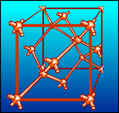
The chemical activity of an atom is determined by the number of electrons in its valence shell. When the valence shell is complete, the atom is stable and shows little tendency to combine with other atoms to form solids. Only atoms that possess eight valence electrons have a complete outer shell. These atoms are referred to as inert or inactive atoms. However, if the valence shell of an atom lacks the required number of electrons to complete the shell, then the activity of the atom increases. Silicon and germanium, for example, are the most frequently used semiconductors. Both are quite similar in their structure and chemical behavior. Each has four electrons in the valence shell. Consider just silicon. Since it has fewer than the required number of eight electrons needed in the outer shell, its atoms will unite with other atoms until eight electrons are shared. This gives each atom a total of eight electrons in its valence shell; four of its own and four that it borrowed from the surrounding atoms. The sharing of valence electrons between two or more atoms produces a COVALENT BOND between the atoms. It is this bond that holds the atoms together in an orderly structure called a CRYSTAL. A crystal is just another name for a solid whose atoms or molecules are arranged in a three-dimensional geometrical pattern commonly referred to as a lattice. Figure 1-7 shows a typical crystal structure. Each sphere in the figure represents the nucleus of an atom, and the arms that join the atoms and support the structure are the covalent bonds. Figure 1-7. - A typical crystal structure.
As a result of this sharing process, the valence electrons are held tightly together. This can best be illustrated by the two-dimensional view of the silicon lattice in figure 1-8. The circles in the figure represent the nuclei of the atoms. The +4 in the circles is the net charge of the nucleus plus the inner shells (minus the valence shell). The short lines indicate valence electrons. Because every atom in this pattern is bonded to four other atoms, the electrons are not free to move within the crystal. As a result of this bonding, pure silicon and germanium are poor conductors of electricity. The reason they are not insulators but semiconductors is that with the proper application of heat or electrical pressure, electrons can be caused to break free of their bonds and move into the conduction band. Once in this band, they wander aimlessly through the crystal. Figure 1-8. - A two-dimensional view of a silicon cubic lattice.
Q.13 What determines the chemical activity of an atom? As stated earlier, energy can be added to electrons by applying heat. When enough energy is absorbed by the valence electrons, it is possible for them to break some of their covalent bonds. Once the bonds are broken, the electrons move to the conduction band where they are capable of supporting electric current. When a voltage is applied to a crystal containing these conduction band electrons, the electrons move through the crystal toward the applied voltage. This movement of electrons in a semiconductor is referred to as electron current flow. There is still another type of current in a pure semiconductor. This current occurs when a covalent bond is broken and a vacancy is left in the atom by the missing valence electron. This vacancy is commonly referred to as a "hole." The hole is considered to have a positive charge because its atom is deficient by one electron, which causes the protons to outnumber the electrons. As a result of this hole, a chain reaction begins when a nearby electron breaks its own covalent bond to fill the hole, leaving another hole. Then another electron breaks its bond to fill the previous hole, leaving still another hole. Each time an electron in this process fills a hole, it enters into a covalent bond. Even though an electron has moved from one covalent bond to another, the most important thing to remember is that the hole is also moving. Therefore, since this process of conduction resembles the movement of holes rather than electrons, it is termed hole flow (short for hole current flow or conduction by holes). Hole flow is very similar to electron flow except that the holes move toward a negative potential and in an opposite direction to that of the electron. Since hole flow results from the breaking of covalent bonds, which are at the valence band level, the electrons associated with this type of conduction contain only valence band energy and must remain in the valence band. However, the electrons associated with electron flow have conduction band energy and can, therefore, move throughout the crystal. A good analogy of hole flow is the movement of a hole through a tube filled with balls (figure 1-9). Figure 1-9. - Analogy of hole flow.
When ball number 1 is removed from the tube, a hole is left. This hole is then filled by ball number 2, which leaves still another hole. Ball number 3 then moves into the hole left by ball number 2. This causes still another hole to appear where ball 3 was. Notice the holes are moving to the right side of the tube. This action continues until all the balls have moved one space to the left in which time the hole moved eight spaces to the right and came to rest at the right-hand end of the tube. In the theory just described, two current carriers were created by the breaking of covalent bonds: the negative electron and the positive hole. These carriers are referred to as electron-hole pairs. Since the semiconductor we have been discussing contains no impurities, the number of holes in the electron-hole pairs is always equal to the number of conduction electrons. Another way of describing this condition where no impurities exist is by saying the semiconductor is INTRINSIC. The term intrinsic is also used to distinguish the pure semiconductor that we have been working with from one containing impurities. Q.15 Name the two types of current flow in a semiconductor. |
 |