Custom Search
|
|
  |
|
|
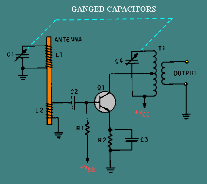
TYPICAL RF AMPLIFIER CIRCUITS As a technician, you will see many different rf amplifiers in many different pieces of equipment. The particular circuit configuration used for an rf amplifier will depend upon how that amplifier is used. In the final part of this chapter, you will be shown some typical rf amplifier circuits. Figure 2-19 is the schematic diagram of a typical rf amplifier that is used in an AM radio receiver. In figure 2-19, the input circuit is the antenna of the radio (L1-a coil) which forms part of an LC circuit which is tuned to the desired station by variable capacitor C1. L1 is wound on the same core as L2, which couples the input signal through C2 to the transistor (Q1). R1 is used to provide proper bias to Q1 from the base power supply (VBB). R2 provides proper bias to the emitter of Q1, and C3 is used to bypass R2. The primary of T1 and capacitor C4 form a parallel LC circuit which acts as the load for Q1. This LC circuit is tuned by C4, which is ganged to C1 allowing the antenna and the LC circuit to be tuned together. The primary of T1 is center-tapped to provide proper impedance matching with Q1. Figure 2-19. - Typical AM radio rf amplifier.
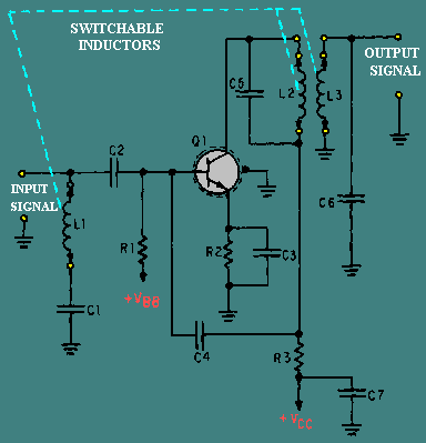
You may notice that no neutralization is shown in this circuit. This circuit is designed for the AM broadcast band (535 kHz - 1605 kHz). At these relatively low rf frequencies the degenerative feedback caused by base-to-collector interelectrode capacitance is minor and, therefore, the amplifier does not need neutralization. Figure 2-20 is a typical rf amplifier used in a vhf television receiver. The input-signal-developing circuit for this amplifier is made up of L1, C1, and C2. The inductor tunes the input-signal-developing circuit for the proper TV channel. (L1 can be switched out of the circuit and another inductor switched in to the circuit by the channel selector.) R1 provides proper bias to Q1 from the base supply voltage (VBB). Q1 is the transistor. Notice that the case of Q1 (the dotted circle around the transistor symbol) is shown to be grounded. The case must be grounded because of the high frequencies (54 MHz - 217 MHz) used by the circuit. R2 provides proper bias from the emitter of Q1, and C3 is used to bypass R2. C5 and L2 are a parallel LC circuit which acts as the load for Q1. The LC circuit is tuned by L2 which is switched in to and out of the LC circuit by the channel selector. L3 and C6 are a parallel LC circuit which develops the signal for the next stage. The parallel LC circuit is tuned by L3 which is switched in to and out of the LC circuit by the channel selector along with L1 and L2. (L1, L2, and L3 are actually part of a bank of inductors. L1, L2, and L3 are in the circuit when the channel selector is on channel 2. For other channels, another group of three inductors would be used in the circuit.) R3 develops a signal which is fed through C4 to provide neutralization. This counteracts the effects of the interelectrode capacitance from the base to the collector of Q1. C7 is used to isolate the rf signal from the collector power supply (VCC). Figure 2-20. - Typical vhf television rf amplifier.
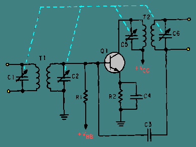
The following questions refer to figure 2-21. Figure 2-21. - Typical rf amplifier.
Q.35 What components form the input-signal-developing impedance for the amplifier? |
 |
|
|
Integrated Publishing, Inc. - A (SDVOSB) Service Disabled Veteran Owned Small Business
|