Custom Search
|
|
  |
|
|
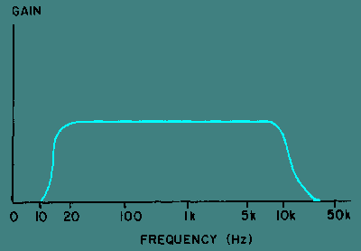
AUDIO AMPLIFIERS An audio amplifier has been described as an amplifier with a Frequency response from 15 Hz to 20 kHz. The Frequency response of an amplifier can be shown graphically with a Frequency response curve. Figure 1-22 is the ideal Frequency response curve for an audio amplifier. This curve is practically "flat" from 15 Hz to 20 kHz. This means that the gain of the amplifier is equal between 15 Hz and 20 kHz. Above 20 kHz or below 15 Hz the gain decreases or "drops off" quite rapidly. The Frequency response of an amplifier is determined by the components in the circuit. Figure 1-22. - Ideal Frequency response curve for an audio amplifier.
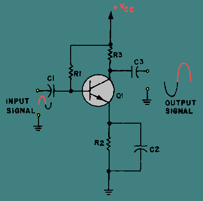
The difference between an audio amplifier and other amplifiers is the frequency response of the amplifier. In the next chapter of this module you will be shown the techniques and components used to change and extend the Frequency response of an amplifier. The transistor itself will respond quite well to the audio frequency range. No special components are needed to extend or modify the Frequency response. You have already been shown the purpose of all the components in a transistor audio amplifier. In this portion of the chapter, schematic diagrams of several audio amplifiers will be shown and the functions of each of the components will be discussed. SINGLE-STAGE AUDIO AMPLIFIERS The first single-stage audio amplifier is shown in figure 1-23 . This circuit is a class A, common-emitter, RC-coupled, transistor, audio amplifier. C1 is a coupling capacitor that couples the input signal to the base of Q1. R1 is used to develop the input signal and provide bias for the base of Q1. R2 is used to bias the emitter and provide temperature stability for Q1. C2 is used to provide decoupling (positive feedback) of the signal that would be developed by R2. R3 is the collector load for Q1 and develops the output signal. C3 is a coupling capacitor that couples the output signal to the next stage. VCC represents the collector-supply voltage. Since the transistor is a common-emitter configuration, it provides voltage amplification. The input and output signals are 180 out of phase. The input and output impedance are both medium. Figure 1-23. - Transistor audio amplifier.
There is nothing new presented in this circuit. You should understand all of the functions of the components in this circuit. If you do not, look back at the various sections presented earlier in this chapter. The second single-stage audio amplifier is shown in figure 1-24 . This circuit is a class A, common-source, RC-coupled, FET, audio amplifier. C1 is a coupling capacitor which couples the input signal to the gate of Q1. R1 is used to develop the input signal for the gate of Q1. R2 is used to bias the source of Q1. C2 is used to decouple the signal developed by R2 (and keep it from affecting the source of Q1). R3 is the drain load for Q1 and develops the output signal. C3 couples the output signal to the next stage. VDD is the supply voltage for the drain of Q1. Since this is a common-source configuration, the input and output signals are 180 out of phase. Figure 1-24. - FET audio amplifier.
If you do not remember how a FET works, refer to NEETS Module 7 Introduction to Solid-State Devices and Power Supplies. The third single-stage audio amplifier is shown in figure 1-25 . This is a class A, common-emitter, transformer-coupled, transistor, audio amplifier. The output device (speaker) is shown connected to the secondary winding of the transformer. C1 is a coupling capacitor which couples the input signal to the base of Q1. R1 develops the input signal. R2 is used to bias the emitter of Q1 and provides temperature stability. C2 is a decoupling capacitor for R2. R3 is used to bias the base of Q1. The primary of T1 is the collector load for Q1 and develops the output signal. T1 couples the output signal to the speaker and provides impedance matching between the output impedance of the transistor (medium) and the impedance of the speaker (low). Figure 1-25. - Single-stage audio amplifier.
Sometimes it is necessary to provide two signals that are equal in amplitude but 180 out of phase with each other. (You will see one use of these two signals a little later in this chapter.) The two signals can be provided from a single input signal by the use of a PHASE SPLITTER. A phase splitter is a device that produces two signals that differ in phase from each other from a single input signal. Figure 1-26 is a block diagram of a phase splitter. Figure 1-26. - Block diagram of a phase splitter.
One way in which a phase splitter can be made is to use a center-tapped transformer. As you may remember from your study of transformers, when the transformer secondary winding is center-tapped, two equal amplitude signals are produced. These signals will be 180 out of phase with each other. So a transformer with a center-tapped secondary fulfills the definition of a phase splitter. A transistor amplifier can be configured to act as a phase splitter. One method of doing this is shown in figure 1-27. Figure 1-27. - Single-stage transistor phase splitter.
C1 is the input signal coupling capacitor and couples the input signal to the base of Q1. R1 develops the input signal. R2 and R3 develop the output signals. R2 and R3 are equal resistances to provide equal amplitude output signals. C2 and C3 couple the output signals to the next stage. R4 is used to provide proper bias for the base of Q1. This phase splitter is actually a single transistor combining the qualities of the common-emitter and common-collector configurations. The output signals are equal in amplitude of the input signal, but are 180 out of phase from each other. If the output signals must be larger in amplitude than the input signal, a circuit such as that shown in figure 1-28 will be used. Figure 1-28 shows a two-stage phase splitter. C1 couples the input signal to the base of Q1. R1 develops the input signal and provides bias for the base of Q1. R2 provides bias and temperature stability for Q1. C2 decouples signals from the emitter of Q1. R3 develops the output signal of Q1. Since Q1 is configured as a common-emitter amplifier, the output signal of Q1 is 180 out of phase with the input signal and larger in amplitude. C3 couples this output signal to the next stage through R4. R4 allows only a small portion of this output signal to be applied to the base of Q2. R5 develops the input signal and provides bias for the base of Q2. R6 is used for bias and temperature stability for Q2. C4 decouples signals from the emitter of Q2. R7 develops the output signal from Q2. Q2 is configured as a common-emitter amplifier, so the output signal is 180 out of phase with the input signal to Q2 (output signal from Q1). The input signal to Q2 is 180 out of phase with the original input signal, so the output from Q2 is in phase with the original input signal. C5 couples this output signal to the next stage. So the circuitry shown provides two output signals that are 180 out of phase with each other. The output signals are equal in amplitude with each other but larger than the input signal. Figure 1-28. - Two-stage transistor phase splitter.
Q.29 What is a phase splitter? |
 |
|
|
Integrated Publishing, Inc. - A (SDVOSB) Service Disabled Veteran Owned Small Business
|