Custom Search
|
|
  |
|
|
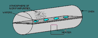
FABRICATION OF IC DEVICES Fabrication of monolithic ICs is the most complex aspect of microelectronic devices we will discuss. Therefore, in this introductory module, we will try to simplify this process as much as possible. Even though the discussion is very basic, the intent is still to increase your appreciation of the progress in microelectronics. You should, as a result of this discussion, come to realize that advances in manufacturing techniques are so rapid that staying abreast of them is extremely difficult. Monolithic Fabrication. Two types of monolithic fabrication will be discussed. These are the DIFFUSION METHOD and the EPITAXIAL METHOD. DIFFUSION METHOD. - The DIFFUSION process begins with the highly polished silicon wafer being placed in an oven (figure 1-11). The oven contains a concentration impurity made up of impurity atoms which yield the desired electrical characteristics. The concentration of impurity atoms is diffused into the wafer and is controlled by controlling the temperature of the oven and the time that the silicon wafer is allowed to remain in the oven. This is called DOPING. When the wafer has been uniformly doped, the fabrication of semiconductor devices may begin. Several hundred circuits are produced simultaneously on the wafer. Figure 1-11. - Wafers in a diffusion oven.
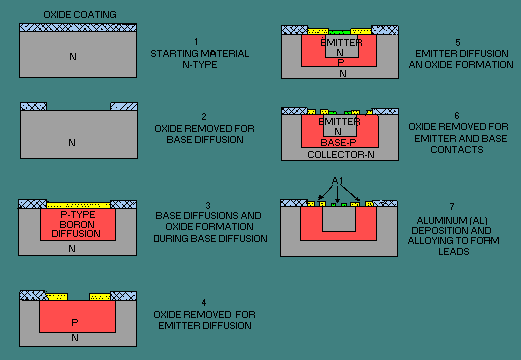
The steps in the fabrication process described here, and illustrated in figure 1-12, would produce an npn, planar-diffused transistor. But, with slight variations, the technique may also be applied to the production of a complete circuit, including diodes, resistors, and capacitors. The steps are performed in the following order: Figure 1-12. - Planar-diffused transistor.
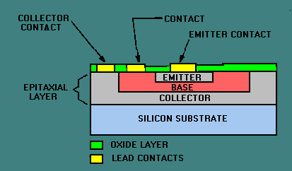
An oxide coating is thermally grown over the n-type silicon starting material. By means of the photolithographic process, a window is opened through the oxide layer. This is done through the use of masks, as discussed earlier. The base of the transistor is formed by placing the wafer in a diffusion furnace containing a p-type impurity, such as boron. By controlling the temperature of the oven and the length of time that the wafer is in the oven, you can control the amount of boron diffused through the window (the boron will actually spread slightly beyond the window opening). A new oxide layer is then allowed to form over the area exposed by the window. A new window, using a different mask much smaller than the first, is opened through the new oxide layer. An n-type impurity, such as phosphorous, is diffused through the new window to form the emitter portion of the transistor. Again, the diffused material will spread slightly beyond the window opening. Still another oxide layer is then allowed to form over the window. By means of precision-masking techniques, very small windows (about 0.005 inch in diameter) are opened in both the base and emitter regions of the transistor to provide access for electrical currents. Aluminum is then deposited in these windows and alloyed to form the leads of the transistor or the IC. (Note that the pn junctions are covered throughout the fabrication process by an oxide layer that prevents contamination.) EPITAXIAL METHOD. - The EPITAXIAL process involves depositing a very thin layer of silicon to form a uniformly doped crystalline region (epitaxial layer) on the substrate. Components are produced by diffusing appropriate materials into the epitaxial layer in the same way as the planar-diffusion method. When planar-diffusion and epitaxial techniques are combined, the component characteristics are improved because of the uniformity of doping in the epitaxial layer. A cross section of a typical planar-epitaxial transistor is shown in figure 1-13. Note that the component parts do not penetrate the substrate as they did in the planar-diffused transistor. Figure 1-13. - Planar-epitaxial transistor.
ISOLATION. - Because of the closeness of components in ICs, ISOLATION from each other becomes a very important factor. Isolation is the prevention of unwanted interaction or leakage between components. This leakage could cause improper operation of a circuit. Techniques are being developed to improve isolation. The most prominent is the use of silicon oxide, which is an excellent insulator. Some manufacturers are experimenting with single-crystal silicon grown on an insulating substrate. Other processes are also used which are far too complex to go into here. With progress in isolation techniques, the reliability and efficiency of ICs will increase rapidly. |
 |
|
|
Integrated Publishing, Inc. - A (SDVOSB) Service Disabled Veteran Owned Small Business
|