Custom Search
|
|
  |
|
|
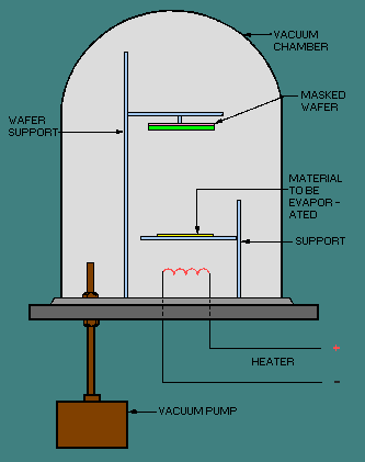
Thin Film Thin film is the term used to describe a technique for depositing passive circuit elements on an insulating substrate with coating to a thickness of 0.0001 centimeter. Many methods of thin-film deposition exist, but two of the most widely used are VACUUM EVAPORATION and CATHODE SPUTTERING. VACUUM EVAPORATION. - Vacuum evaporation is a method used to deposit many types of materials in a highly evacuated chamber in which the material is heated by electricity, as shown in figure 1-14. The material is radiated in straight lines in all directions from the source and is shadowed by any objects in its path. Figure 1-14. - Vacuum evaporation oven.
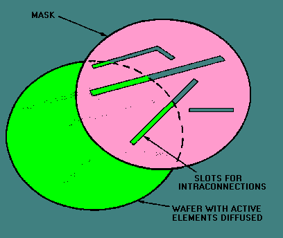
The wafers, with appropriate masks (figure 1-15), are placed above and at some distance from the material being evaporated. When the process is completed, the vacuum is released and the masks are removed from the wafers. This process leaves a thin, uniform film of the deposition material on all parts of the wafers exposed by the open portions of the mask. This process is also used to deposit interconnections (leads) between components of an IC. Figure 1-15. - Evaporation mask.
The vacuum evaporation technique is most suitable for deposition of highly reactive materials, such as aluminum, that are difficult to work with in air. The method is clean and allows a better contact between the layer of deposited material and the surface upon which it has been deposited. In addition, because evaporation beams travel in straight lines, very precise patterns may be produced. CATHODE-SPUTTERING. - A typical cathode-sputtering system is illustrated in figure 1-16. This process is also performed in a vacuum. A potential of 2 to 5 kilovolts is applied between the anode and cathode (source material). This produces a GLOW DISCHARGE in the space between the electrodes. The rate at which atoms are SPUTTERED off the source material depends on the number of ions that strike it and the number of atoms ejected for each ion bombardment. The ejected atoms are deposited uniformly over all objects within the chamber. When the sputtering cycle is completed, the vacuum in the chamber is released and the wafers are removed. The masks are then removed from the wafers, leaving a deposit that forms the passive elements of the circuit, as shown in figure 1-17. Figure 1-16. - Cathode-sputtering system.
Figure 1-17. - Cathode-sputtering mask.
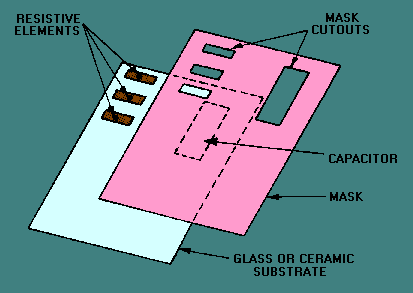
Finely polished glass, glazed ceramic, and oxidized silicon have been used as substrate materials for thin films. A number of materials, including nichrome, a compound of silicon oxide and chromium cermets, tantalum, and titanium, have been used for thin-film resistors. Nichrome is the most widely used. The process for producing thin-film capacitors involves deposition of a bottom electrode, a dielectric, and finally a top electrode. The most commonly used dielectric materials are silicon monoxide and silicon dioxide. Thick Film Thick films are produced by screening patterns of conducting and insulating materials on ceramic substrates. A thick film is a film of material with a thickness that is at least 10 times greater than the mean free path of an electron in that material, or approximately 0.001 centimeter. The technique is used to produce only passive elements, such as resistors and capacitors. PROCEDURES. - One procedure used in fabricating a thick film is to produce a series of stencils called SCREENS. The screens are placed on the substrate and appropriate conducting or insulating materials are wiped across the screen. Once the conducting or insulating material has been applied, the screens are removed and the formulations are fired at temperatures above 600 degrees Celsius. This process forms alloys that are permanently bonded to the insulating substrate. To a limited extent, the characteristics of the film can be controlled by the firing temperature and length of firing time. RESISTORS. - Thick-film resistance values can be held to a tolerance of 10 percent. Closer tolerances are obtained by trimming each resistor after fabrication. Hundreds of different cermet formulations are used to produce a wide range of component parameters. For example, the material used for a 10-ohm-per-square resistor is quite different from that used for a 100-kilohm-per-square resistor. CAPACITORS AND RESISTOR-CAPACITOR NETWORKS. - Capacitors are formed by a sequence of screenings and firings. Capacitors in this case consist of a bottom plate, intraconnections, a dielectric, and a top plate. For resistor-capacitor networks, the next step would be to deposit the resistor material through the screen. The final step is screening and firing of a glass enclosure to seal the unit. Hybrid Microcircuit A hybrid microcircuit is one that is fabricated by combining two or more circuit types, such as film and semiconductor circuits, or a combination of one or more circuit types and discrete elements. The primary advantage of hybrid microcircuits is design flexibility; that is, hybrid microcircuits can be designed to provide wide use in specialized applications, such as low-volume and high-frequency circuits. Several elements and circuits are available for hybrid applications. These include discrete components that are electrically and mechanically compatible with ICs. Such components may be used to perform functions that are supplementary to those of ICs. They can be handled, tested, and assembled with essentially the same technology and tools. A hybrid IC showing an enlarged chip is shown in figure 1-18. Figure 1-18. - Hybrid IC showing an enlarged chip.
Complete circuits are available in the form of UNCASED CHIPS (UNENCAPSULATED IC DICE). These chips are usually identical to those sold as part of the manufacturer's regular production line. They must be properly packaged and connected by the user if a high-quality final assembly is to be obtained. The circuits are usually sealed in a package to protect them from mechanical and environmental stresses. One-mil (0.001-inch), gold-wire leads are connected to the appropriate pins which are brought out of the package to allow external connections. Q.22 Name the two types of monolithic IC construction discussed. |
|
|
|
Integrated Publishing, Inc. - A (SDVOSB) Service Disabled Veteran Owned Small Business
|