Custom Search
|
|
  |
|
|
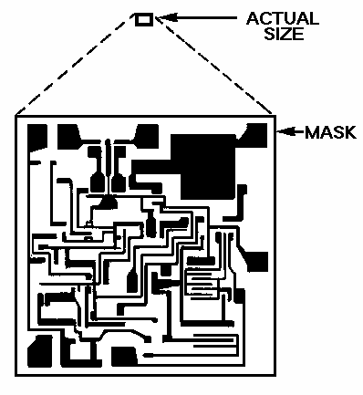
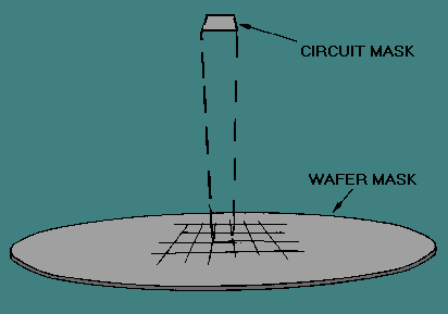
FABRICATION OF MICROELECTRONIC DEVICES The purpose of this section is to give you a simplified overview of the manufacture of microelectronic devices. The process is far more complex than will be described here. Still, you will be able to see that microelectronics is not magic, but a highly developed technology. Development of a microelectronic device begins with a demand from industry or as the result of research. A device that is needed by industry may be a simple diode network or a complex circuit consisting of thousands of components. No matter how complex the device, the basic steps of production are similar. Each type of device requires circuit design, component arrangement, preparation of a substrate, and the depositing of proper materials on the substrate. The first consideration in the development of a new device is to determine what the device is to accomplish. Once this has been decided, engineers can design the device. During the design phase, the engineers will determine the numbers and types of components and the interconnections, needed to complete the planned circuit. COMPONENT ARRANGEMENT Planning the component arrangement for a microelectronic device is a very critical phase of production. Care must be taken to ensure the most efficient use of space available. With simple devices, this can be accomplished by hand. In other words, the engineers can prepare drawings of component placement. However, a computer is used to prepare the layout for complex devices. The computer is able to store the characteristics of thousands of components and can provide a printout of the most efficient component placement. Component placement is then transferred to extremely large drawings. During this step, care is taken to maintain the patterns as they will appear on the substrate. Figure 1-7 shows a fairly simple IC MASK PATTERN. If this pattern were being prepared for production, it would be drawn several hundred times the size shown and then photographed. The photo would then be reduced in size until it was the actual desired size. At that time, the pattern would be used to produce several hundred patterns that would be used on one substrate. Figure 1-8 illustrates how the patterns would be distributed to act as a WAFER MASK for manufacturing. Figure 1-7. - IC mask pattern.
Figure 1-8. - Wafer mask distribution.
A wafer mask is a device used to deposit materials on a substrate. It allows material to be deposited in certain areas, but not in others. By changing the pattern of the mask, we can change the component arrangement of the circuit. Several different masks may be used to produce a simple microelectronic device. When used in proper sequence, conductor, semiconductor, or insulator materials may be applied to the substrate to form transistors, resistors, capacitors, and interconnecting leads. As was mentioned earlier in this topic, microelectronic devices are produced on a substrate. This substrate will be of either insulator or semiconductor material, depending on the type of device. Film and hybrid ICs are normally constructed on a glass or ceramic substrate. Ceramic is usually the preferred material because of its durability. Substrates used in monolithic ICs are of semiconductor material, usually silicon. In this type of IC, the substrate can be an active part of the IC. Glass or ceramic substrates are used only to provide support for the components. Semiconductor substrates are produced by ARTIFICIALLY GROWING cylindrical CRYSTALS of pure silicon or germanium. Crystals are "grown" on a SEED CRYSTAL from molten material by slowly lifting and cooling the material repeatedly. This process takes place under rigidly controlled atmospheric and temperature conditions. Figure 1-9 shows a typical CRYSTAL FURNACE. The seed crystal is lowered until it comes in contact with the molten material-silicon in this case. It is then rotated and raised very slowly. The seed crystal is at a lower temperature than the molten material. When the molten material is in contact with the seed, it solidifies around the seed as the seed is lifted. This process continues until the grown crystal is of the desired length. A typical crystal is about 2 inches in diameter and 10 to 12 inches long. Larger diameter crystals can be grown to meet the needs of the industry. The purity of the material is strictly controlled to maintain specific semiconductor properties. Depending on the need, n or p impurities are added to produce the desired characteristics. Several other methods of growing crystals exist, but the basic concept of crystal production is the same. Figure 1-9. - Crystal furnace.
The cylinder of semiconductor material that is grown is sliced into thicknesses of .010 to .020 inch in the first step of preparation, as shown in figure 1-10. These wafers are ground and polished to remove any irregularities and to provide the smoothest surface possible. Although both sides are polished, only the side that will receive the components must have a perfect finish. Figure 1-10. - Silicon crystal and wafers.
Q.17 What are the basic steps in manufacturing an IC? |
 
|
|
|
Integrated Publishing, Inc. - A (SDVOSB) Service Disabled Veteran Owned Small Business
|