Custom Search
|
|
  |
|||||||||||||||||||||||||||||||||||||
|
SUMMARY Now that you have completed this chapter, a short review of the more important points covered in the chapter will follow. This review should refresh your memory of transistors, their theory of operation, and how they are tested with an ohmmeter. A TRANSISTOR is a three or more element solid-state device that amplifies by controlling the flow of current carriers through its semiconductor materials.
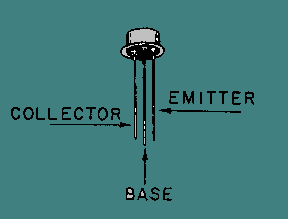
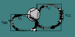
The THREE ELEMENTS OF A TRANSISTOR are (1) the EMITTER, which gives off current carriers, (2) the BASE, which controls the carriers, and (3) the COLLECTOR, which collects the carriers.
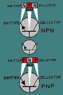
The two BASIC TYPES OF TRANSISTORS are the NPN and PNP. The only difference in symbology between the two transistors is the direction of the arrow on the emitter. If the arrow points in, it is a PNP transistor and if it points outward , it is an NPN transistor.
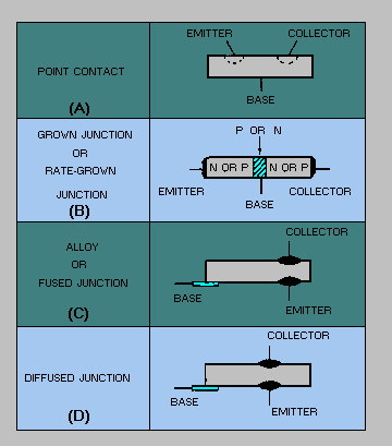
The four TRANSISTOR MANUFACTURING PROCESSES are the (1) point contact, (2) grown or rate-grown junction, (3) alloy or fused junction, and (4) diffused junction.
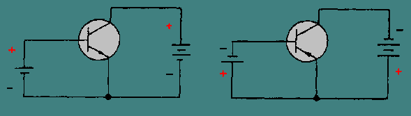
The PROPER BIASING OF A TRANSISTOR enables the transistor to be used as an amplifier. To function in this capacity, the emitter-to-base junction of the transistor is forward biased, while the base-to-collector junction is reverse biased.
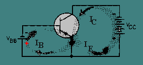
NPN TRANSISTOR OPERATION is basically the action of a relatively small emitter-base bias voltage controlling a relatively large emitter-to-collector current.
PNP TRANSISTOR OPERATION is essentially the same as the NPN operation except the majority current carriers are holes and the bias batteries are reversed.
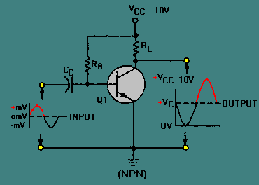
AMPLIFICATION is the process of increasing the strength of a signal. An AMPLIFIER is the device that provides amplification without appreciably altering the original signal. The BASIC TRANSISTOR AMPLIFIER amplifies by producing a large change in collector current for a small change in base current. This action results in voltage amplification because the load resistor placed in series with the collector reacts to these large changes in collector current which, in turn, results in large variations in the output voltage.
The three types of BIAS used to properly bias a transistor are base-current bias (fixed bias), self-bias, and combination bias. Combination bias is the one most widely used because it improves circuit stability and at the same time overcomes some of the disadvantages of base-current bias and self-bias.
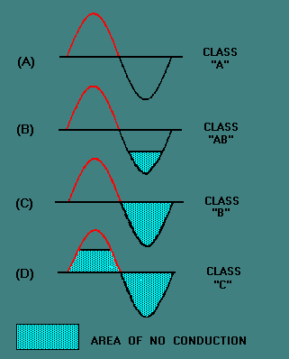
THE CLASS OF AMPLIFIER OPERATION is determined by the portion of the input signal for which there is an output. There are four classes of amplifier operations: class A, class AB, class B, and class C.
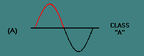
CUTOFF occurs when the base-to-emitter bias prevents current from flowing in the emitter circuit. For example, in the PNP transistor, if the base becomes positive with respect to the emitter, holes are repelled at the emitter-base junction. This prevents current from flowing in the collector circuit. SATURATION occurs in a PNP transistor when the base becomes so negative, with respect to the emitter, that changes in the signal are not reflected in collector-current flow. CLASS A AMPLIFIERS are biased so that variations in input signal polarities occur within the limits of cutoff and saturation. Biasing an amplifier in this manner allows collector current to flow during the complete cycle (360 degrees) of the input signal, thus providing an output which is a replica of the input but 180 degrees out of phase. Class A operated amplifiers are used as audio- and radio-frequency amplifiers in radio, radar, and sound systems.
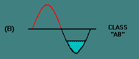
CLASS AB AMPLIFIERS are biased so that collector current is zero (cutoff) for a portion of one alternation of the input signal. Therefore, collector current will flow for more than 180 degrees but less than 360 degrees of the input signal. The class AB amplifier is commonly used as a push-pull amplifier to overcome a side effect of class B operations.
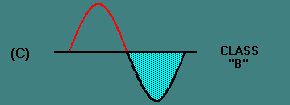
CLASS B AMPLIFIERS are biased so that collector current is cut off during one-half of the input signal. Thus, for a class B operation, collector current will flow for approximately 180 degrees (half) of the input signal. The class B operated amplifier is used as an audio amplifier and sometimes as the driver- and power-amplifier stage of transmitters.
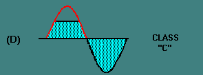
CLASS C AMPLIFIERS are biased so that collector current flows for less than one-half cycle of the input signal. The class C operated amplifier is used as a radio-frequency amplifier in transmitters.
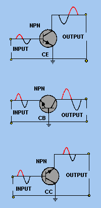
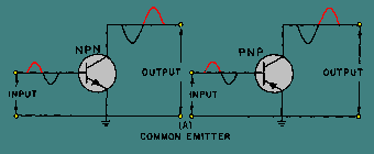
FIDELITY and EFFICIENCY are two terms used in conjunction with amplifiers. Fidelity is the faithful reproduction of a signal, while efficiency is the ratio of output signal power compared to the total input power. The class A amplifier has the highest degree of fidelity, but the class C amplifier has the highest efficiency. A TRANSISTOR CONFIGURATION is the particular way a transistor is connected in a circuit. A transistor may be connected in any one of three different configurations: common emitter (CE), common base (CB), and common collector (CC).
The COMMON-EMITTER CONFIGURATION (CE) is the most frequently used configuration in practical amplifier circuits, since it provides good voltage, current, and power gain. The input to the CE is applied to the base-emitter circuit and the output is taken from the collector-emitter circuit, making the emitter the element "common" to both input and output. The CE is set apart from the other configurations, because it is the only configuration that provides a phase reversal between input and output signals.
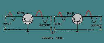
The COMMON-BASE CONFIGURATION (CB) is mainly used for impedance matching, since it has a low input resistance and a high output resistance. It also has a current gain of less than 1. In the CB, the input is applied to the emitter, the output is taken from the collector, and the base is the element common to both input and output.
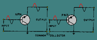
The COMMON-COLLECTOR CONFIGURATION (CC) is used as a current driver for impedance matching and is particularly useful in switching circuits. The CC is also referred to as an emitter-follower and is equivalent to the electron-tube cathode follower. Both have high input impedance and low output impedance. In the CC, the input is applied to the base, the output is taken from the emitter, and the collector is the element common to both input and output.
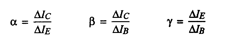
GAIN is a term used to describe the amplification capabilities of an amplifier. It is basically a ratio of output to input. The current gain for the three transistor configurations (CB, CE, and CC) are ALPHA ( a), BETA (b), and GAMMA (g), respectively.
The TRANSISTOR CONFIGURATION COMPARISON CHART gives a rundown of the different properties of the three configurations.
TRANSISTOR CHARACTERISTICS are usually presented on specification sheets. These sheets usually cover the following items:
TRANSISTORS ARE IDENTIFIED by a Joint Army-Navy (JAN) designation printed directly on the case of the transistor. If in doubt about a transistor's markings, always replace a transistor with one having identical markings, or consult an equipment or transistor manual to ensure that an identical replacement or substitute is used.
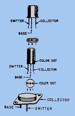
TESTING A TRANSISTOR to determine if it is good or bad can be done with an ohmmeter or transistor tester or by the substitution method. PRECAUTIONS should be taken when working with transistors since they are susceptible to damage by electrical overloads, heat, humidity, and radiation. TRANSISTOR LEAD IDENTIFICATION plays an important part in transistor maintenance because before a transistor can be tested or replaced, its leads must be identified. Since there is NO standard method of identifying transistor leads, check some typical lead identification schemes or a transistor manual before attempting to replace a transistor.
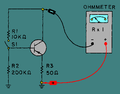
A TRANSISTOR GAIN TEST can be made using an ohmmeter and a simple test circuit. The principle behind this test lies in the fact that little or no current will flow in a transistor between emitter and collector until the emitter-base junction is forward biased. A 10-to-1 resistance ratio in the test between meter readings indicates normal gain.
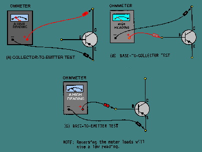
TRANSISTOR JUNCTION RESISTANCE TEST can also be made using an ohmmeter by measuring the base-emitter, base-collector, and collector-emitter forward and reverse resistances.
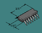
MICROELECTRONICS is a broad term used to describe the use of integrated circuits to miniaturize electronic equipment. A PRINTED CIRCUIT BOARD (PCB) is a flat, insulating surface upon which printed wiring and miniaturized components are connected in a predetermined design and attached to a common base. MODULAR CIRCUITRY is an assembly technique in which printed circuit boards are stacked and connected together to form a module. This technique increases the packaging density of circuit components and results in a considerable reduction in the size of electronic equipment. An INTEGRATED CIRCUIT is a device that integrates (combines) both active components (transistors, diodes, etc.) and passive components (resistors, capacitors, etc.) of a complete electronic circuit in a single chip.
The two basic types of ICs are the HYBRID and the MONOLITHIC. In the MONOLITHIC IC, all elements (resistors, transistors, etc.) associated with the circuit are fabricated inseparably with a continuous piece of material (called the substrate). In the HYBRID IC, the passive components (resistors, capacitors) are deposited onto a substrate (foundation) made of glass, ceramic, or other insulating material. Then the active components (diodes, transistors) are attached to the substrate and connected to the passive components using fine wire. |
 |
||||||||||||||||||||||||||||||||||||