Custom Search
|
|
  |
|
|
Up to now the various semiconductors, resistors, capacitors, etc., in our discussions have been considered as separately packaged components, called DISCRETE COMPONENTS. In this section we will introduce some of the more complex devices that contain complete circuits packaged as a single component. These devices are referred to as INTEGRATED CIRCUITS and the broad term used to describe the use of these devices to miniaturize electronic equipment is called MICROELECTRONICS. With the advent of the transistor and the demand by the military for smaller equipment, design engineers set out to miniaturize electronic equipment. In the beginning, their efforts were frustrated because most of the other components in a circuit such as resistors, capacitors, and coils were larger than the transistor. Soon these other circuit components were miniaturized, thereby pushing ahead the development of smaller electronic equipment. Along with miniature resistors, capacitors, and other circuit elements, the production of components that were actually smaller than the space required for the interconnecting wiring and cabling became possible. The next step in the research process was to eliminate these bulky wiring components. This was accomplished with the PRINTED CIRCUIT BOARD (PCB). A printed circuit board is a flat insulating surface upon which printed wiring and miniaturized components are connected in a predetermined design, and attached to a common base. Figure 2-20 (view A and view B) shows a typical printed circuit board. Notice that various components are connected to the board and the printed wiring is on the reverse side. With this technique, all interconnecting wiring in a piece of equipment, except for the highest power leads and cabling, is reduced to lines of conducting material (copper, silver, gold, etc.) deposited directly on the surface of an insulating "circuit board." Since printed circuit boards are readily adapted as plug-in units, the elimination of terminal boards, fittings and tie points, not to mention wires, results in a substantial reduction in the overall size of electronic equipment. Figure 2-20A. - A typical printed circuit board (PCB). FRONT SIDE
Figure 2-20B. - A typical printed circuit board (PCB). REVERSE SIDE
After the printed circuit boards were perfected, efforts to miniaturize electronic equipment were then shifted to assembly techniques, which led to MODULAR CIRCUITRY. In this technique, printed circuit boards are stacked and connected together to form a module. This increases the packaging density of circuit components and results in a considerable reduction in the size of electronic equipment. Since the module can be designed to perform any electronic function, it is also a very versatile unit. However, the drawback to this approach was that the modules required a considerable number of connections that took up too much space and increased costs. In addition, tests showed the reliability was adversely affected by the increase in the number of connections. A new technique was required to improve reliability and further increase packaging density. The solution was INTEGRATED CIRCUITS. An integrated circuit is a device that integrates (combines) both active components (transistors, diodes, etc.) and passive components (resistors, capacitors, etc.) of a complete electronic circuit in a single chip (a tiny slice or wafer of semiconductor crystal or insulator). Integrated circuits (ICs) have almost eliminated the use of individual electronic components (resistors, capacitors, transistors, etc.) as the building blocks of electronic circuits. Instead, tiny CHIPS have been developed whose functions are not that of a single part, but of dozens of transistors, resistors, capacitors, and other electronic elements, all interconnected to perform the task of a complex circuit. Often these comprise a number of complete conventional circuit stages, such as a multistage amplifier (in one extremely small component). These chips are frequently mounted on a printed circuit board, as shown in figure 2-21, which plugs into an electronic unit. Figure 2-21. - ICs on a printed circuit board.
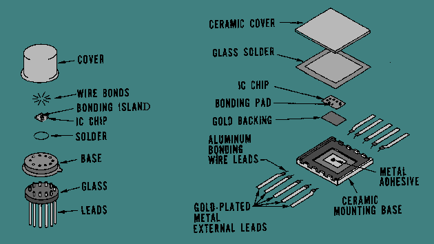
Integrated circuits have several advantages over conventional wired circuits of discrete components. These advantages include (1) a drastic reduction in size and weight, (2) a large increase in reliability, (3) lower cost, and (4) possible improvement in circuit performance. However, integrated circuits are composed of parts so closely associated with one another that repair becomes almost impossible. In case of trouble, the entire circuit is replaced as a single component. Basically, there are two general classifications of integrated circuits: HYBRID and MONOLITHIC. In the monolithic integrated circuit, all elements (resistors, transistors, etc.) associated with the circuit are fabricated inseparably within a continuous piece of material (called the SUBSTRATE), usually silicon. The monolithic integrated circuit is made very much like a single transistor. While one part of the crystal is being doped to form a transistor, other parts of the crystal are being acted upon to form the associated resistors and capacitors. Thus, all the elements of the complete circuit are created in the crystal by the same processes and in the same time required to make a single transistor. This produces a considerable cost savings over the same circuit made with discrete components by lowering assembly costs. Hybrid integrated circuits are constructed somewhat differently from the monolithic devices. The PASSIVE components (resistors, capacitors) are deposited onto a substrate (foundation) made of glass, ceramic, or other insulating material. Then the ACTIVE components (diodes, transistors) are attached to the substrate and connected to the passive circuit components on the substrate using very fine (.001 inch) wire. The term hybrid refers to the fact that different processes are used to form the passive and active components of the device. Hybrid circuits are of two general types: (1) thin film and (2) thick film. "Thin" and "thick" film refer to the relative thickness of the deposited material used to form the resistors and other passive components. Thick film devices are capable of dissipating more power, but are somewhat more bulky. Integrated circuits are being used in an ever increasing variety of applications. Small size and weight and high reliability make them ideally suited for use in airborne equipment, missile systems, computers, spacecraft, and portable equipment. They are often easily recognized because of the unusual packages that contain the integrated circuit. A typical packaging sequence is shown in figure 2-22. These tiny packages protect and help dissipate heat generated in the device. One of these packages may contain one or several stages, often having several hundred components. Some of the most common package styles are shown in figure 2-23. Figure 2-22. - A typical integrated circuit packaging sequence.
Figure 2-23. - Common IC packaging styles.
The preceding information was presented to give you a brief introduction into integrated circuits. If you wish to pursue this subject further, additional information is available in your ship's or station's library. |
 |