Custom Search
|
|
  |
|
|
DUAL-DIODE LIMITER The last type of limiter to be discussed in this chapter is the DUAL-DIODE LIMITER, shown in figure 4-15, view (A). This limiter combines a parallel-negative limiter with negative bias (D1 and B1) and a parallel-positive limiter with positive bias (D2 and B2). Parts of both the positive and negative alternations are removed in this circuit. Each battery aids the reverse bias of the diode in its circuit; the circuit has no current flow with no input signal. When the input signal is below the value of the biasing batteries, both D1 and D2 are reverse biased. With D1 and D2 reverse biased, the output follows the input. When the input signal becomes more positive than +20 volts (view (B)), D2 conducts and limits the output to +20 volts. When the input signal becomes more negative than -20 volts, D1 conducts and limits the output to this, value. When neither diode conducts, the output follows the input waveform. Figure 4-15A. - Dual-diode limiter.
Figure 4-15B. - Dual-diode limiter.
CLAMPERS Certain applications in electronics require that the upper or lower extremity of a wave be fixed at a specific value. In such applications, a CLAMPING (or CLAMPER) circuit is used. A clamping circuit clamps or restrains either the upper or lower extremity of a waveform to a fixed dc potential. This circuit is also known as a DIRECT-CURRENT RESTORER or a BASE-LINE STABILIZER. Such circuits are used in test equipment, radar systems, electronic countermeasure systems, and sonar systems. Depending upon the equipment, you could find negative or positive clampers with or without bias. Figure 4-16, views (A ) through (E), illustrates some examples of waveforms created by clampers. However, before we discuss clampers, we will review some relevant points about series RC circuits. Figure 4-16A. - Clamping waveforms. WITHOUT CLAMPING
Figure 4-16B. - Clamping waveforms. WITH CLAMPING, LOWER EXTREMITY OF WAVE IS HELD AT 0V
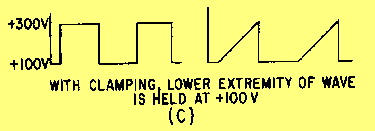
Figure 4-16C. - Clamping waveforms. WITH CLAMPING, LOWER EXTREMITY OF WAVE IS HELD AT +100 V
Figure 4-16D. - Clamping waveforms. WITH CLAMPING, UPPER EXTREMITY OF WAVE IS HELD AT 0V
Figure 4-16E. - Clamping waveforms. WITH CLAMPING, UPPER EXTREMITY OF WAVE IS HELD AT -100 V
SERIES RC CIRCUITS Series RC circuits are widely used for coupling signals from one stage to another. If the time constant of the coupling circuit is comparatively long, the shape of the output waveform will be almost identical to that of the input. However, the output dc reference level may be different from that of the input. Figure 4-17, view (A), shows a typical RC coupling circuit in which the output reference level has been changed to 0 volts. In this circuit, the values of R1 and C1 are chosen so that the capacitor will charge (during T0 to T1) to 20 percent of the applied voltage, as shown in view (B). With this in mind, let's consider the operation of the circuit. Figure 4-17A. - RC coupling.
Figure 4-17B. - RC coupling.
At T0 the input voltage is -50 volts and the capacitor begins charging. At the first instant the voltage across C is 0 and the voltage across R is -50 volts. As C charges, its voltage increases. The voltage across R, which is the output voltage, begins to drop as the voltage across C increases. At T1 the capacitor has charged to 20 percent of the -50 volts input, or -10 volts. Because the input voltage is now 0 volts, the capacitor must discharge. It discharges through the low impedance of the signal source and through R, developing +10 volts across R at the first instant. C discharges 20 percent of the original 10-volt charge from T1 to T2. Thus, C discharges to +8 volts and the output voltage also drops to 8 volts. At T2 the input signal becomes -50 volts again. This -50 volts is in series opposition to the 8-volt charge on the capacitor. Thus, the voltage across R totals -42 volts (-50 plus +8 volts). Notice that this value of voltage (-42 volts) is smaller in amplitude than the amplitude of the output voltage which occurred at TO (-50 volts). Capacitor C now charges from +8 to +16 volts. If we were to continue to follow the operation of the circuit, we would find that the output wave shape would become exactly distributed around the 0-volt reference point. At that time the circuit operation would have reached a stable operating point. Note that the output wave shape has the same amplitude and approximately the same shape as the input wave shape, but now "rides" equally above and below 0 volts. Clampers use this RC time so that the input and output waveforms will be almost identical, as shown from T11 to T12. |
|
|
|
Integrated Publishing, Inc. - A (SDVOSB) Service Disabled Veteran Owned Small Business
|