Custom Search
|
|
  |
|
|
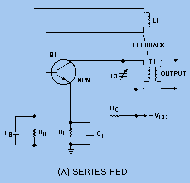
OSCILLATOR CIRCUITS Oscillators may be classified by name, such as Armstrong, Hartley, Colpitts, or by the manner in which dc power is applied. An oscillator in which dc power is supplied to the transistor through the tank circuit, or a portion of the tank circuit, is said to be SERIES FED. An oscillator which receives its dc power for the transistor through a path separate and parallel to the tank circuit is said to be PARALLEL FED OR SHUNT FED. All the oscillators in this chapter can be constructed either way, series or shunt fed. The construction depends on the characteristics of the oscillator circuit the designer is interested in. A SERIES-FED, TUNED-COLLECTOR ARMSTRONG OSCILLATOR is illustrated in figure 2-9 , view (A). The dc path is from the negative side (ground) of VCC through RE, Q1, T1, and back to the positive side of VCC. The figure clearly illustrates that both the ac and dc components flow through the tank circuit. Figure 2-9A. - Series- and shunt-fed, tuned-collector Armstrong oscillators. SERIES-FED
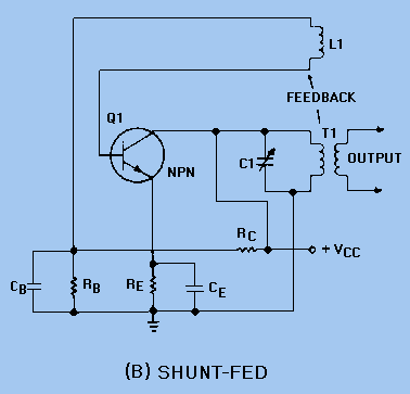
By modifying the circuit slightly, it becomes a SHUNT-FED, TUNED-COLLECTOR ARMSTRONG OSCILLATOR as shown in view (B). The dc component flows from ground through RE to Q1 to positive VCC. The dc is blocked from the tank circuit by capacitor C2. Only the ac component flows in the tank circuit. Figure 2-9B. - Series- and shunt-fed, tuned-collector Armstrong oscillators. SHUNT-FED
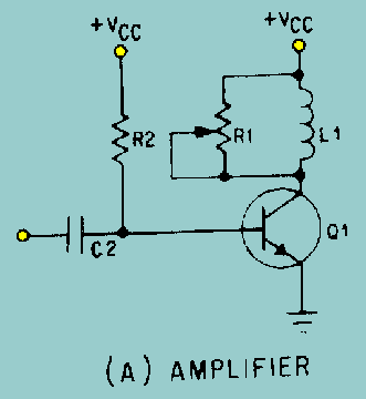
The function of an oscillator is to produce a sinusoidal waveshape of a specific frequency and amplitude. In doing so, the stability of an oscillator is very important. Depending on its application, an oscillator may be required to have either good frequency stability or amplitude stability; in many circumstances, both are required. Of the two, good frequency stability is usually considered more important. FREQUENCY STABILITY The FREQUENCY STABILITY of an oscillator is a measure of the degree to which a constant frequency output is approached. The better the frequency stability, the closer the output will be to a constant frequency. Frequency INSTABILITY (variations above and below the desired output frequency) may be caused by transistor characteristics or by variations in the external circuit elements. As stated before, when output power is not of prime importance, transistor oscillators may be biased class A to ensure stability and minimize distortion. When this is done, the dc operating point established by the power supply is chosen so that the operation of the transistor oscillator occurs over the most linear portion of the transistor's characteristic curve. When the operation of the circuit falls into the nonlinear portion of the characteristic curve, the transistor's parameters (voltages and currents) vary. These parameters are basic to the stable frequency of the transistor oscillator. Operating frequency variations may occur with changes in these bias voltages. Thus, a constant supply voltage is a prime requirement for good frequency stability. The use of a common bias source for both collector and emitter electrodes results in a relatively constant ratio of the two voltages. In effect, a change in one voltage is somewhat counteracted by the change in the other. This counteraction takes place because an increase in collector voltage causes an increase in the oscillating frequency, and an increase in emitter voltage causes a decrease in the oscillating frequency. This is a result of the change in capacitance between the junctions of the transistor. However, a common bias source does not completely compensate since the effects on other circuit parameters of each bias voltage differ. Just as in any transistor circuit, changes in the transistor operating point and changes in temperature are encountered in the transistor oscillator. The effects of changes in temperature are to cause collector current to increase if the transistor is not stabilized. The increase in collector current can be prevented by reducing the forward bias. AMPLITUDE STABILITY The AMPLITUDE STABILITY of a transistor oscillator indicates the amount by which the actual output amplitude varies from the desired output amplitude. The same parameters (voltages and currents) that affect frequency stability also affect amplitude stability. Output amplitude may be kept relatively constant by ensuring that the feedback is large enough that the collector current is maintained at the proper level. Feedback used in this manner makes the output voltage directly proportional to the supply voltage. Thus, regulation of the supply voltage ensures good amplitude stability. ARMSTRONG OSCILLATOR The ARMSTRONG OSCILLATOR is used to produce a sine-wave output of constant amplitude and of fairly constant frequency within the rf range. It is generally used as a local oscillator in receivers, as a source in signal generators, and as a radio-frequency oscillator in the medium- and high-frequency range. The identifying characteristics of the Armstrong oscillator are that (1) it uses an LC tuned circuit to establish the frequency of oscillation, (2) feedback is accomplished by mutual inductive coupling between the tickler coil and the LC tuned circuit, and (3) it uses a class C amplifier with self-bias. Its frequency is fairly stable, and the output amplitude is relatively constant. Views (A), (B), and (C) shown in figure 2-10 can be used to build the basic Armstrong oscillator. View (A) shows a conventional amplifier. R2 provides the forward bias for Q1, C2 is a coupling capacitor, and L1 and R1 form the collector load impedance. This is a common-emitter configuration which provides the 180-degree phase shift between the base and collector. Figure 2-10A. - Basic Armstrong oscillator circuit. AMPLIFIER
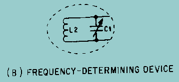
Figure 2-10B. - Basic Armstrong oscillator circuit. FREQUENCY-DETERMINING DEVICE
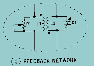
Figure 2-10C. - Basic Armstrong oscillator circuit. FEEDBACK NETWORK
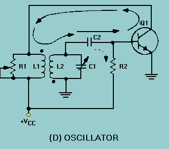
Figure 2-10D. - Basic Armstrong oscillator circuit. OSCILLATOR
View (B)shows the frequency-determining device composed of inductor L2 and capacitor C1. C1 is a variable tuning capacitor which is used to adjust the resonant frequency to the desired value. View (C) is the feedback network which uses L1 (the collector load) as the primary and L2 as the secondary winding of a coupling transformer to provide a 180-degree phase shift. Variable resistor R1 controls the amount of current through L1. When R1 is adjusted for maximum resistance, most of the current flows through L1. The transformer now couples a maximum signal which represents a large feedback amplitude into the tank circuit (L2, C1). If R1 is adjusted for a smaller resistance, less current flows through L1, and less energy is coupled to the tank circuit; therefore, feedback amplitude decreases. R1 is normally adjusted so that the L1 current is adequate to sustain tank oscillations. View (D) shows the complete oscillator circuit. Connecting the feedback network through coupling capacitor C2 to the base of Q1 forms a "closed loop" for feedback (shown by the solid arrows). Let's verify that the feedback is regenerative. Assume a positive signal on the base of Q1. The transistor conducts heavily when forward biased. This current flow through L1 and R1 causes the voltage across L1 to increase. The voltage increase is inductively coupled to L2 and inverted. This action ensures that the voltage is positive at the base end of L2 and C1 and in phase with the base voltage. The positive signal is now coupled through C2 to the base of Q1. The regenerative feedback offsets the damping in the frequency-determining network and has sufficient amplitude to provide unity circuit gain. |
 |
|
|
Integrated Publishing, Inc. - A (SDVOSB) Service Disabled Veteran Owned Small Business
|