Custom Search
|
|
  |
|
|
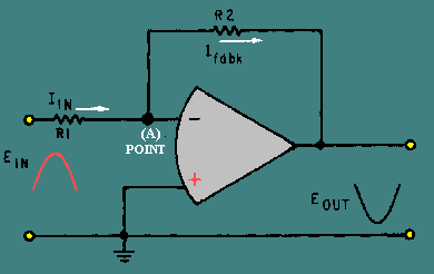
You can compute the values for view (C) and prove that point A in that circuit is also at virtual ground. The whole point is that the inverting input to the operational amplifier shown in figure 3-13 is at virtual ground since it is at 0 volts (for all practical purposes). Because the inverting input is at 0 volts, there will be no current (for all practical purposes) flowing into the operational amplifier from the connection point of R1 and R2. Given these conditions, the characteristics of this circuit are determined almost entirely by the values of R1 and R2. Figure 3-15 should help show how the values of R1 and R2 determine the circuit characteristics. Figure 3-15. - Current flow in the operational circuit.
NOTE: It should be stressed at this point that for purpose of explanation the operational amplifier is a theoretically perfect amplifier. In actual practice we are dealing with less than perfect. In the practical operational amplifier there will be a slight input current with a resultant power loss. This small signal can be measured at the theoretical point of virtual ground. This does not indicate faulty operation. The input signal causes current to flow through R1. (Only the positive half cycle of the input signal is shown and will be discussed.) Since the voltage at the inverting input of the operational amplifier is at 0 volts, the input current (Iin) is computed by:
The output signal (which is opposite in phase to the input signal) causes a feedback current (Ifdbk) to flow through R2. The left-hand side of R2 is at 0 volts (point A) and the right-hand side is at Eout. Therefore, the feedback current is computed by:
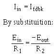
(The minus sign indicates that Eout is 180 degrees out of phase with Ein and should not be confused with output polarity.) Since no current flows into or out of the inverting input of the operational amplifier, any current reaching point A from R1 must flow out of point A through R2. Therefore, the input current (Iin) and the feedback current (Ifdbk) must be equal. Now we can develop a mathematical relationship between the input and output signals and R1 and R2. Mathematically:
If you multiply both sides of the equation by R1:
If you divide both sides of the equation by Eout:
By inverting both sides of the equation:
You should recall that the voltage gain of a stage is defined as the output voltage divided by the input voltage:
Therefore, the voltage gain of the inverting configuration of the operational amplifier is expressed by the equation:
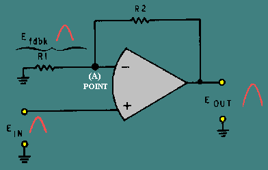
(As stated earlier, the minus sign indicates that the output signal is 180 degrees out of phase with the input signal.) Noninverting Configuration Figure 3-16 shows a noninverting configuration using an operational amplifier. The input signal (Ein) is applied directly to the noninverting (+) input of the operational amplifier. Feedback is provided by coupling part of the output signal (Eout) back to the inverting (-) input of the operational amplifier. R1 and R2 act as voltage divider that allows only a part of the output signal to be applied as feedback (Efdbk). Figure 3-16. - Noninverting configuration.
Notice that the input signal, output signal, and feedback signal are all in phase. (Only the positive alternation of the signal is shown.) It may appear as if the feedback is regenerative (positive) because the feedback and input signals are in phase. The feedback is, in reality, degenerative (negative) because the input signals is applied to the noninverting input and the feedback signal is applied to the inverting input, (Remember, that the operational amplifier will react to the difference between the two inputs.) Just as in the inverting configuration, the feedback signal is equal to the input signal (for all practical purposes). This time, however, the feedback signal is in phase with the input signal. Therefore:
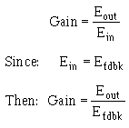
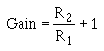
Given this condition, you can calculate the gain of the stage in terms of the resistors (R1 and R2). The gain of the stage is defined as:
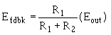
The feedback signal (Efdbk) can be shown in terms of the output signal (Eout) and the voltage divider (R1 and R2). The voltage divider has the output signal on one end and ground (0 volts) on the other end. The feedback signal is that part of the output signal developed by R1 (at point A). Another way to look at it is that the feedback signal is the amount of output signal left (at point A) after part of the output signal has been dropped by R2. In either case, the feedback signal (Efdbk) is the ratio of R1 to the entire voltage divider (R1 + R2) multiplied by the output signal (Eout). Mathematically, the relationship of the output signal, feedback signal, and voltage divider is:
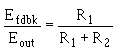
If you divide both sides of the equation by Eout:
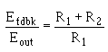
By inverting both sides of the equation:
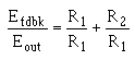
Separating the right-hand side:
Remember:
Therefore, by substitution:
You can now see that the gain of the noninverting configuration is determined by the resistors. The formula is different from the one used for the inverting configuration, but the gain is still determined by the values of R1 and R2. |
 
|
|
|
Integrated Publishing, Inc. - A (SDVOSB) Service Disabled Veteran Owned Small Business
|