Custom Search
|
|
  |
|
|
SPECIAL AMPLIFIERS LEARNING OBJECTIVES
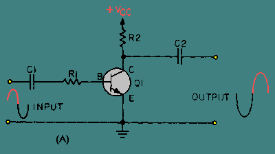
INTRODUCTION If you were to make a quick review of the subjects discussed in this module up to this point, you would see that you have been given a considerable amount of information about amplifiers. You have been shown what amplification is and how the different classes of amplifiers affect amplification. You also have been shown that many factors must be considered when working with amplifiers, such as impedance, feedback, Frequency response, and coupling. With all this information behind you, you might ask yourself "what more can there be to know about amplifiers?" There is a great deal more to learn about amplifiers. Even after you finish this chapter you will have only "scratched the surface" of the study of amplifiers. But, you will have prepared yourself for the remainder of the NEETS. This, in turn, should prepare you for further study and, perhaps, a career in electronics. As in chapter 2, the circuits shown in this chapter are intended to present particular concepts to you. Therefore, the circuits may be incomplete or not practical for use in an actual piece of electronic equipment. You should keep in mind the fact that this text is intended to teach certain facts about amplifiers, and in order to simplify the illustrations used, complete operational circuits are not always shown. In this chapter three types of special amplifiers are discussed. These are: DIFFERENTIAL AMPLIFIERS, OPERATIONAL AMPLIFIERS, and MAGNETIC AMPLIFIERS. These are called special amplifiers because they are used only in certain types of equipment. The names of each of these special amplifiers describe the operation of the amplifier, NOT what is amplified. For example, a magnetic amplifier does not amplify magnetism but uses magnetic effects to produce amplification of an electronic signal. A differential amplifier is an amplifier that can have two input signals and/or two output signals. This amplifier can amplify the difference between two input signals. A differential amplifier will also "cancel out" common signals at the two inputs. One of the more interesting aspects of an operational amplifier is that it can be used to perform mathematical operations electronically. Properly connected, an operational amplifier can add, subtract, multiply, divide, and even perform the calculus operations of integration and differentiation. These amplifiers were originally used in a type of computer known as the "analog computer" but are now used in many electronic applications. The magnetic amplifier uses a device called a "saturable core reactor" to control an a.c.output signal. The primary use of magnetic amplifiers is in power control systems. These brief descriptions of the three special amplifiers are intended to provide you with a general idea of what these amplifiers are and how they can be used. The remaining sections of this chapter will provide you with more detailed information on these special amplifiers. A differential amplifier has two possible inputs and two possible outputs. This arrangement means that the differential amplifier can be used in a variety of ways. Before examining the three basic configurations that are possible with a differential amplifier, you need to be familiar with the basic circuitry of a differential amplifier. BASIC DIFFERENTIAL AMPLIFIER CIRCUIT Before you are shown the operation of a differential amplifier, you will be shown how a simpler circuit works. This simpler circuit, known as the DIFFERENCE AMPLIFIER, has one thing in common with the differential amplifier: It operates on the difference between two inputs. However, the difference amplifier has only one output while the differential amplifier can have two outputs. By now, you should be familiar with some amplifier circuits, which should give you an idea of what a difference amplifier is like. In NEETS, module 7, you were shown the basic configurations for transistor amplifiers. Figure 3-1 shows two of these configurations: the common emitter and the common base. In view (A) of figure 3-1 a common-emitter amplifier is shown. The output signal is an amplified version of the input signal and is 180 degrees out of phase with the input signal. View (B) is a common-base amplifier. In this circuit the output signal is an amplified version of the input signal and is in phase with the input signal. In both of these circuits, the output signal is controlled by the base-to-emitter bias. As this bias changes (because of the input signal) the current through the transistor changes. This causes the output signal developed across the collector load (R2) to change. None of this information is new, it is just a review of what you have already been shown regarding transistor amplifiers. Figure 3-1A. - Common-emitter and common-base amplifiers.
Figure 3-1B. - Common-emitter and common-base amplifiers.
NOTE: Bias arrangements for the following explanations will be termed base-to-emitter. In other publications you will see the term emitter-to-base used to describe the same bias arrangement. THE TWO-INPUT, SINGLE-OUTPUT, DIFFERENCE AMPLIFIER If you combine the common-base and common-emitter configurations into a single transistor amplifier, you will have a circuit like the one shown in figure 3-2. This circuit is the two-input, single-output, difference amplifier. Figure 3-2. - Two-input, single-output, difference amplifier.
In figure 3-2, the transistor has two inputs (the emitter and the base) and one output (the collector). Remember, the current through the transistor (and therefore the output signal) is controlled by the base-to-emitter bias. In the circuit shown in figure 3-2, the combination of the two input signals controls the output signal. In fact, the DIFFERENCE BETWEEN THE INPUT SIGNALS determines the base-to-emitter bias. For the purpose of examining the operation of the circuit shown in figure 3-2, assume that the circuit has a gain of -10. This means that for each 1-volt change in the base-to-emitter bias, there would be a 10-volt change in the output signal. Assume, also, that the input signals will peak at 1-volt levels (+1 volt for the positive peak and -1 volt for the negative peak). The secret to understanding this circuit (or any transistor amplifier circuit) is to realize that the collector current is controlled by the base-to-emitter bias. In other words, in this circuit the output signal (the voltage developed across R3) is determined by the difference between the voltage on the base and the voltage on the emitter. Figure 3-3 shows this two-input, single-output amplifier with input signals that are equal in amplitude and 180 degrees out of phase. Input number one has a positive alternation when input number two has a negative alternation and vice versa. Figure 3-3. - Input signals 180 out of phase.
The circuit and the input and output signals are shown at the top of the figure. The lower portion of the figure is a comparison of the input signals and the output signal. Notice the vertical lines marked "T0" through "T8." These represent "time zero" through "time eight." In other words, these lines provide a way to examine the two input signals and the output signal at various instants of time. In figure 3-3 at time zero (T0) both input signals are at 0 volts. The output signal is also at 0 volts. Between time zero (T0) and time one (T1), input signal number one goes positive and input signal number two goes negative. Each of these voltage changes causes an increase in the base-to-emitter bias which causes current through Q1 to increase. Increased current through Q1 results in a greater voltage drop across the collector load (R3) which causes the output signal to go negative. By time one (T1), input signal number one has reached +1 volt and input signal number two has reached -1 volt. This is an overall increase in base-to-emitter bias of 2 volts. Since the gain of the circuit is -10, the output signal has decreased by 20 volts. As you can see, the output signal has been determined by the difference between the two input signals. In fact, the base-to-emitter bias can be found by subtracting the value of input signal number two from the value of input signal number one.
Between time one (T1) and time two (T2), input signal number one goes from +1 volt to 0 volts and input signal number two goes from -1 volt to 0 volts. At time two (T2) both input signals are at 0 volts and the base-to-emitter bias has returned to 0 volts. The output signal is also 0 volts.
Between time two (T2) and time three (T3), input signal number one goes negative and input signal number two goes positive. At time three (T3), the value of the base-to-emitter bias is -2 volts.
This causes the output signal to be +20 volts at time three (T3). Between time three (T3) and time four (T4), input signal #1 goes from -1 volt to 0 volts and input signal #2 goes from +1 volt to 0 volts. At time four (T4) both input signals are 0 volts, the bias is 0 volts, and the output is 0 volts. During time four (T4) through time eight (T8), the circuit repeats the sequence of events that took place from time zero (T0) through time four (T4). You can see that when the input signals are equal in amplitude and 180 degrees out of phase, the output signal is twice as large (40 volts peak to peak) as it would be from either input signal alone (if the other input signal were held at 0 volts). |
 |
|
|
Integrated Publishing, Inc. - A (SDVOSB) Service Disabled Veteran Owned Small Business
|