Custom Search
|
|
  |
|
|
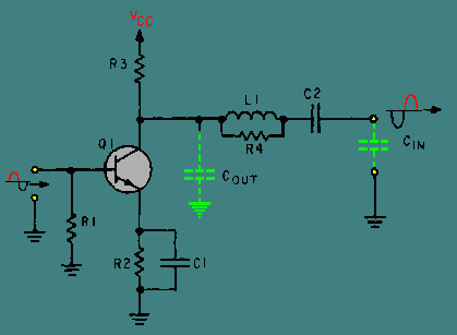
VIDEO AMPLIFIERS As you have seen, a transistor amplifier is limited in its Frequency response. You should also remember from chapter 1 that a VIDEO AMPLIFIER should have a frequency response of 10 hertz (10 Hz) to 6 megahertz (6 MHz). The question has probably occurred to you: How is it possible to "extend" the range of Frequency response of an amplifier? HIGH-FREQUENCY COMPENSATION FOR VIDEO AMPLIFIERS If the frequency-response range of an audio amplifier must be extended to 6 megahertz (6 MHz) for use as a video amplifier, some means must be found to overcome the limitations of the audio amplifier. As you have seen, the capacitance of an amplifier circuit and the interelectrode capacitance of the transistor (or electronic tube) cause the higher Frequency response to be limited. In some ways capacitance and inductance can be thought of as opposites. As stated before, as frequency increases, capacitive reactance decreases, and inductive reactance increases. Capacitance opposes changes in voltage, and inductance opposes changes in current. Capacitance causes current to lead voltage, and inductance causes voltage to lead current. Since frequency affects capacitive reactance and inductive reactance in opposite ways, and since it is the capacitive reactance that causes the problem with high-frequency response, inductors are added to an amplifier circuit to improve the high-frequency response. This is called HIGH-FREQUENCY COMPENSATION. Inductors (coils), when used for high-frequency compensation, are called PEAKING COILS. Peaking coils can be added to a circuit so they are in series with the output signal path or in parallel to the output signal path. Instead of only in series or parallel, a combination of peaking coils in series and parallel with the output signal path can also be used for high-frequency compensation. As in all electronic circuits, nothing comes free. The use of peaking coils WILL increase the Frequency response of an amplifier circuit, but it will ALSO lower the gain of the amplifier. Series Peaking The use of a peaking coil in series with the output signal path is known as SERIES PEAKING. Figure 2-6 shows a transistor amplifier circuit with a series peaking coil. In this figure, R1 is the input-signal-developing resistor. R2 is used for bias and temperature stability of Q1. C1 is the bypass capacitor for R2. R3 is the load resistor for Q1 and develops the output signal. C2 is the coupling capacitor which couples the output signal to the next stage. "Phantom" capacitor COUT represents the output capacitance of the circuit, and "phantom" capacitor CIN represents the input capacitance of the next stage. Figure 2-6. - Series peaking coil.
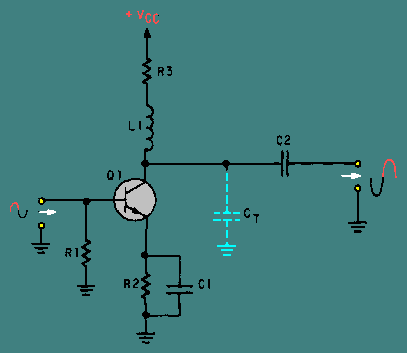
You know that the capacitive reactance of COUT and CIN will limit the high-Frequency response of the circuit. L1 is the series peaking coil. It is in series with the output-signal path and isolates COUT from CIN. R4 is called a "swamping" resistor and is used to keep L1 from overcompensating at a narrow range of frequencies. In other words, R4 is used to keep the frequency-response curve flat. If R4 were not used with L1, there could be a "peak" in the frequency-response curve. (Remember, L1 is called a peaking coil.) Shunt Peaking If a coil is placed in parallel (shunt) with the output signal path, the technique is called SHUNT PEAKING. Figure 2-7 shows a circuit with a shunt peaking coil. With the exceptions of the "phantom" capacitor and the inductor, the components in this circuit are the same as those in figure 2-6. R1 is the input-signal-developing resistor. R2 is used for bias and temperature stability. C1 is the bypass capacitor for R2. R3 is the load resistor for Q1 and develops the output signal. C2 is the coupling capacitor which couples the output signal to the next stage. Figure 2-7. - Shunt peaking coil.
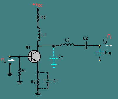
The "phantom" capacitor, CT, represents the total capacitance of the circuit. Notice that it tends to couple the output signal to ground. L1 is the shunt peaking coil. While it is in series with the load resistor (R3), it is in parallel (shunt) with the output-signal path. Since inductive reactance increases as frequency increases, the reactance of L1 develops more output signal as the frequency increases. At the same time, the capacitive reactance of CT is decreasing as frequency increases. This tends to couple more of the output signal to ground. The increased inductive reactance counters the effect of the decreased capacitive reactance and this increases the high-Frequency response of the amplifier. Combination Peaking You have seen how a series peaking coil isolates the output capacitance of an amplifier from the input capacitance of the next stage. You have also seen how a shunt peaking coil will counteract the effects of the total capacitance of an amplifier. If these two techniques are used together, the combination is more effective than the use of either one alone. The use of both series and shunt peaking coils is known as COMBINATION PEAKING. An amplifier circuit with combination peaking is shown in figure 2-8. In figure 2-8 the peaking coils are L1 and L2. L1 is a shunt peaking coil, and L2 is a series peaking coil. Figure 2-8. - Combination peaking.
The "phantom" capacitor CT represents the total capacitance of the amplifier circuit. "Phantom" capacitor CIN represents the input capacitance of the next stage. Combination peaking will easily allow an amplifier to have a high-Frequency response of 6 megahertz (6 MHz). Q.8 What is the major factor that limits the high-Frequency response of an amplifier
circuits? |
|
|
|
Integrated Publishing, Inc. - A (SDVOSB) Service Disabled Veteran Owned Small Business
|