Custom Search
|
|
  |
|
|
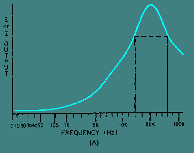
Figure 2-3A. - Frequency-response curves for Q3.
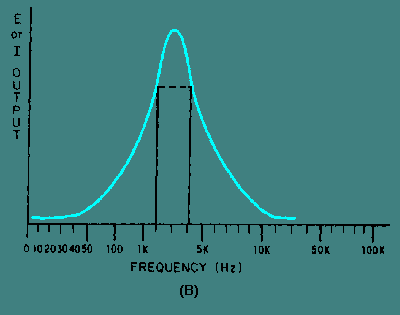
Figure 2-3B. - Frequency-response curves for Q3.
FACTORS AFFECTING Frequency response OF AN AMPLIFIER In chapter 1 of this module, the fact was mentioned that an audio amplifier is limited in its Frequency response. Now you will see why this is true. You should recall that the Frequency response of an a.c. circuit is limited by the reactive elements (capacitance and inductance) in the circuit. As you know, this is caused by the fact that the capacitive and inductive reactances vary with the frequency. In other words, the value of the reactance is determined, in part, by frequency. Remember the formulas:
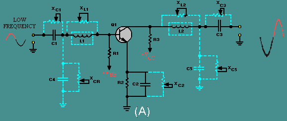
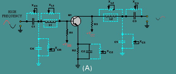
If you ignore the amplifying device (transistor, electron tube, etc.), and if the amplifier circuit is made up of resistors only, there should be no limits to the frequency response. In other words, a totally resistive circuit would have no frequency limits. However, there is no such thing as a totally resistive circuit because circuit components almost always have some reactance. In addition to the reactance of other components in the circuit, most amplifiers use RC coupling. This means that a capacitor is used to couple the signal in to and out of the circuit. There is also a certain amount of capacitance and inductance in the wiring of the circuit. The end result is that all circuits are reactive. To illustrate this point, figure 2-4 shows amplifier circuits with the capacitance and inductance of the wiring represented as "phantom" capacitors and inductors. The reactances of the capacitors (XC) and the inductors (XL) are shown as "phantom" variable resistors. View (A) shows the circuit with a low-frequency input signal, and view (B) shows the circuit with a high-frequency input signal. Figure 2-4A. - Amplifiers showing reactive elements and reactance.
Figure 2-4B. - Amplifiers showing reactive elements and reactance.
The actual circuit components are: C1, C2, C3, R1, R2, R3, and Q1. C1 is used to couple the input signal. R1 develops the input signal. R2, the emitter resistor, is used for proper biasing and temperature stability. C2 is a decoupling capacitor for R2. R3 develops the output signal. C3 couples the output signal to the next stage. Q1 is the amplifying device. The phantom circuit elements representing the capacitance and inductance of the wiring are: L1, L2, C4, and C5. L1 represents the inductance of the input wiring. L2 represents the inductance of the output wiring. C4 represents the capacitance of the input wiring. C5 represents the capacitance of the output wiring. In view (A) the circuit is shown with a low-frequency input signal. Since the formulas for capacitive reactance and inductive reactance are
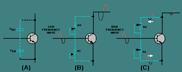
you should remember that if frequency is low, capacitive reactance will be high and inductive reactance will be low. This is shown by the position of the variable resistors that represent the reactances. Notice that XL1 and XL2 are low; therefore, they do not "drop" very much of the input and output signals. XC4 and XC5 are high; these reactances tend to "block" the input and output signals and keep them from going to the power supplies (VBB and VCC). Notice that the output signal is larger in amplitude than the input signal. Now look at view (B). The input signal is a high-frequency signal. Now XC is low and XL is high. XL1 and XL2 now drop part of the input and output signals. At the same time XC4 and XC5 tend to "short" or "pass" the input and output signals to signal ground. The net effect is that both the input and output signals are reduced. Notice that the output signal is smaller in amplitude than the input signal. Now you can see how the capacitance and inductance of the wiring affect an amplifier, causing the output of an amplifier to be less for high-frequency signals than for low-frequency signals. In addition to the other circuit components, an amplifying device (transistor or electronic tube), itself, reacts differently to high frequencies than it does to low frequencies. In earlier NEETS modules you were told that transistors and electronic tubes have interelectrode capacitance. Figure 2-5 shows a portion of the interelectrode capacitance of a transistor and the way in which this affects high- and low-frequency signals. Figure 2-5. - Interelectrode capacitance of a transistor.
In view (A) a transistor is shown with phantom capacitors connected to represent the interelectrode capacitance. CEB represents the emitter-to-base capacitance. CBC represents the base-to-collector capacitance. For simplicity, in views (B) and (C) the capacitive reactance of these capacitors is shown by variable resistors R1 (for CEB) and R2 (for CBC). View (B) shows the reactance as high when there is a low-frequency input signal. In this case there is very little effect from the reactance on the transistor. The transistor amplifies the input signal as shown in view (B). However, when a high-frequency input signal is applied to the transistor, as in view (C), things are somewhat different. Now the capacitive reactance is low (as shown by the settings of the variable resistors). In this case, as the base of the transistor attempts to go positive during the first half of the input signal, a great deal of this positive signal is felt on the emitter (through R1). If both the base and the emitter go positive at the same time, there is no change in emitter-base bias and the conduction of the transistor will not change. Of course, a small amount of change does occur in the emitter-base bias, but not as much as when the capacitive reactance is higher (at low frequencies). As an output signal is developed in the collector circuit, part of this signal is fed back to the base through R2. Since the signal on the collector is 180 degrees out of phase with the base signal, this tends to drive the base negative. The effect of this is to further reduce the emitter-base bias and the conduction of the transistor.During the second half of the input signal, the same effect occurs although the polarity is reversed. The net effect is a reduction in the gain of the transistor as indicated by the small output signal. This decrease in the amplifier output at higher frequencies is caused by the interelectrode capacitance. (There are certain special cases in which the feedback signal caused by the interelectrode capacitance is in phase with the base signal. However, in most cases, the feedback caused by interelectrode capacitance is degenerative and is 180 degrees out of phase with the base signal as explained above.) Q.4 What are the factors that limit the Frequency response of a transistor amplifier? |
|
|
|
Integrated Publishing, Inc. - A (SDVOSB) Service Disabled Veteran Owned Small Business
|