Custom Search
|
|
  |
|
|
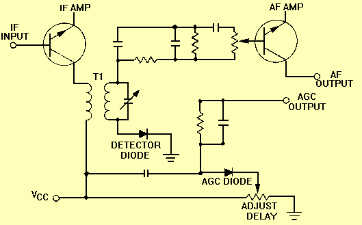
Delayed Automatic Gain Control The disadvantage of automatic gain control, attenuating even the weak signal, is overcome by the use of delayed automatic gain control (dagc). Let's take a look at the typical dagc circuitry in figure 2-19. This type of system develops no agc feedback until an established received signal strength is attained. For signals weaker than this value, no agc is developed. For sufficiently strong signals, the delayed agc circuit operates essentially the same as ordinary agc. Figure 2-19. - Delayed agc action.
Our circuit uses two separate diodes; one is the detector diode and the other the agc diode. The agc diode is connected to the primary of the last IF transformer and the detector diode to its secondary. A positive bias is applied to the cathode of the agc diode. This keeps it from conducting until a prearranged signal level has been reached. The adjust delay control allows manual control of the agc diode bias. Manual control allows you to select the signal level at which agc is applied. If mostly weak stations are to be received, the setting should be high (no agc until the signal level is high). However, you should set it as low as possible to prevent overloading of the last IF amplifier by stronger signals. Finally, you must have two diodes to obtain delayed agc. If only one diode were used, the agc would be developed from the detector diode, and there would be no delayed action. Or, if a signal diode were biased to provide the delaying action desired, no signal would pass to the audio amplifier until the bias was exceeded by the input signal. Beat-Frequency Oscillator The beat-frequency oscillator (bfo) is necessary when you want to receive cw signals. Cw signals are not modulated with an audio component, you remember, so we must provide one. The action of the rf amplifier, mixer, local oscillator, and IF amplifier is the same for both cw and AM; but the cw signal reaches the detector as a single frequency signal with no sideband components. To produce an af output, you must heterodyne (beat) any cw signal with an rf signal of the proper frequency. This separate signal is obtained from an oscillator known as a beat-frequency oscillator. Figure 2-20 is a block diagram of a superheterodyne receiver capable of receiving and demodulating a cw signal. The bfo heterodynes at the detector and produces an af output. The detector (second detector) is used primarily because the mixer (first detector) is normally used as the source of agc. Figure 2 - 20. - Placement of the beat frequency oscillator.
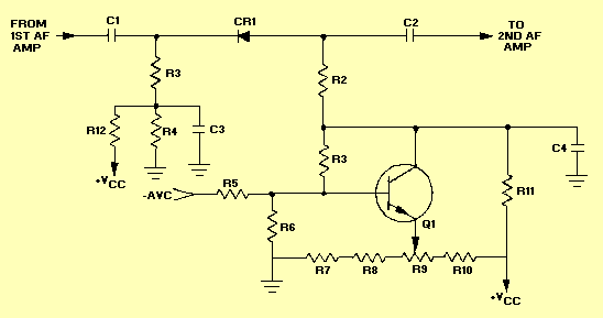
If the intermediate frequency is 455 kilohertz and the bfo is tuned to 456 kilohertz or 454 kilohertz, the difference frequency of 1 kilohertz is heard in the output. Generally, you will tune the bfo from the front panel of a receiver. When you vary the bfo control, you are varying the output frequency of the bfo and will hear changes in the tone of the output audio signal. Squelch The sensitivity of a receiver is maximum when no signal is being received. This condition occurs, for example, when a receiver is being tuned between stations. At this time background noise is picked up by the antenna, and you will hear noise greatly amplified. This noise is highly annoying and occurs because receiver gain is maximum without a signal. You can often overcome this problem by using a circuit called a SQUELCH, NOISE SILENCER, NOISE SUPPRESSOR, or NOISE LIMITER. All of these noise type circuits just clip the peaks of the noise spikes. Squelch will actually eliminate noise. Figure 2-21 is a typical circuit of this type. The circuit cuts off receiver output when no input signal is being received. It accomplishes this by blocking either the detector or audio amplifier when no signal is present. Let's take a look at the theory involved in this process. Figure 2-21. - Squelch circuit.
The squelch diode CR1 connects the output of the first af stage to the input of the second. Amplifier Q1 serves as the control transistor for the circuit. The anode and cathode voltages of CR1 are normally biased positive with respect to ground. With no input signal, R9 is adjusted until Q1 draws enough collector current to reduce its collector voltage and the anode voltage of CR1 to a value below the voltage on the cathode of CR1. At this point the anode voltage of the squelch diode is negative with respect to its cathode, and conduction ceases. Audio output is now reduced to zero and the receiver is silent. The base of Q1 is connected to the automatic volume control (avc) line. Anytime a signal enters the receiver, a negative avc voltage is applied to the base of Q1. This reduces the collector current and increases the collector voltage, which in turn increases the anode voltage of CR1 until the anode becomes positive with respect to the cathode. Once again diode CR1 will conduct, and the signal will be passed to the second af amplifier. Diode CR1 is effectively a switch controlled by the avc voltage. Q.19 What is a disadvantage of agc? |
 |
|
|
Integrated Publishing, Inc. - A (SDVOSB) Service Disabled Veteran Owned Small Business
|