Custom Search
|
|
  |
|
|
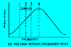
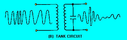
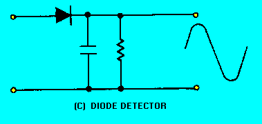
FM DEMODULATION In fm demodulators, the intelligence to be recovered is not in amplitude variations; it is in the variation of the instantaneous frequency of the carrier, either above or below the center frequency. The detecting device must be constructed so that its output amplitude will vary linearly according to the instantaneous frequency of the incoming signal. Several types of fm detectors have been developed and are in use, but in this section you will study three of the most common: (1) the phase-shift detector, (2) the ratio detector, and (3) the gated-beam detector. To be able to understand the principles of operation for fm detectors, you need to first study the simplest form of frequency-modulation detector, the SLOPE DETECTOR. The slope detector is essentially a tank circuit which is tuned to a frequency either slightly above or below the fm carrier frequency. View (A) of figure 3-9 is a plot of voltage versus frequency for a tank circuit. The resonant frequency of the tank is the frequency at point 4. Components are selected so that the resonant frequency is higher than the frequency of the fm carrier signal at point 2. The entire frequency deviation for the fm signal falls on the lower slope of the bandpass curve between points 1 and 3. As the fm signal is applied to the tank circuit in view (B), the output amplitude of the signal varies as its frequency swings closer to, or further from, the resonant frequency of the tank. Frequency variations will still be present in this waveform, but it will also develop amplitude variations, as shown in view (B). This is because of the response of the tank circuit as it varies with the input frequency. This signal is then applied to the diode detector in view (C) and the detected waveform is the output. This circuit has the major disadvantage that any amplitude variations in the rf waveform will pass through the tank circuit and be detected. This disadvantage can be eliminated by placing a limiter circuit before the tank input. (Limiter circuits were discussed in NEETS, Module 9, Introduction to Wave-Generation and Wave-Shaping Circuits.) This circuit is basically the same as an AM detector with the tank tuned to a higher or lower frequency than the received carrier. Figure 3-9A. - Slope detector. VOLTAGE VERSUS FREQUENCY PLOT
Figure 3-9B. - Slope detector. TANK CIRCUIT
Figure 3-9C. - Slope detector. DIODE DETECTOR
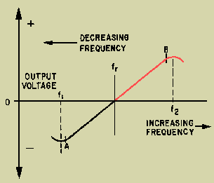
Q.21 What is the simplest form of fm detector? FOSTER-SEELEY DISCRIMINATOR The FOSTER-SEELEY DISCRIMINATOR is also known as the PHASE-SHIFT DISCRIMINATOR. It uses a double-tuned rf transformer to convert frequency variations in the received fm signal to amplitude variations. These amplitude variations are then rectified and filtered to provide a dc output voltage. This voltage varies in both amplitude and polarity as the input signal varies in frequency. A typical discriminator response curve is shown in figure 3-10. The output voltage is 0 when the input frequency is equal to the carrier frequency (fr). When the input frequency rises above the center frequency, the output increases in the positive direction. When the input frequency drops below the center frequency, the output increases in the negative direction. Figure 3-10. - Discriminator response curve.
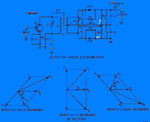
The output of the Foster-Seeley discriminator is affected not only by the input frequency, but also to a certain extent by the input amplitude. Therefore, using limiter stages before the detector is necessary. Circuit Operation of a Foster-Seeley Discriminator View (A) of figure 3-11 shows a typical Foster-Seeley discriminator. The collector circuit of the preceding limiter/amplifier circuit (Q1) is shown. The limiter/amplifier circuit is a special amplifier circuit which limits the amplitude of the signal. This limiting keeps interfering noise low by removing excessive amplitude variations from signals. The collector circuit tank consists of C1 and L1. C2 and L2 form the secondary tank circuit. Both tank circuits are tuned to the center frequency of the incoming fm signal. Choke L3 is the dc return path for diode rectifiers CR1 and CR2. R1 and R2 are not always necessary but are usually used when the back (reverse bias) resistance of the two diodes is different. Resistors R3 and R4 are the load resistors and are bypassed by C3 and C4 to remove rf. C5 is the output coupling capacitor. Figure 3-11. - Foster-Seeley discriminator. FOSTER-SEELEY DISCRIMINATOR
CIRCUIT OPERATION AT RESONANCE. - The operation of the Foster-Seeley discriminator can best be explained using vector diagrams [figure 3-11, view (B)] that show phase relationships between the voltages and currents in the circuit. Let's look at the phase relationships when the input frequency is equal to the center frequency of the resonant tank circuit. The input signal applied to the primary tank circuit is shown as vector ep. Since coupling capacitor C8 has negligible reactance at the input frequency, rf choke L3 is effectively in parallel with the primary tank circuit. Also, because L3 is effectively in parallel with the primary tank circuit, input voltage ep also appears across L3. With voltage ep applied to the primary of T1, a voltage is induced in the secondary which causes current to flow in the secondary tank circuit. When the input frequency is equal to the center frequency, the tank is at resonance and acts resistive. Current and voltage are in phase in a resistance circuit, as shown by is and ep. The current flowing in the tank causes voltage drops across each half of the balanced secondary winding of transformer T1. These voltage drops are of equal amplitude and opposite polarity with respect to the center tap of the winding. Because the winding is inductive, the voltage across it is 90 degrees out of phase with the current through it. Because of the center-tap arrangement, the voltages at each end of the secondary winding of T1 are 180 degrees out of phase and are shown as e1 and e2 on the vector diagram. The voltage applied to the anode of CR1 is the vector sum of voltages ep and e1, shown as e3 on the diagram. Likewise, the voltage applied to the anode of CR2 is the vector sum of voltages ep and e2, shown as e4 on the diagram. At resonance e3 and e4 are equal, as shown by vectors of the same length. Equal anode voltages on diodes CR1 and CR2 produce equal currents and, with equal load resistors, equal and opposite voltages will be developed across R3 and R4. The output is taken across R3 and R4 and will be 0 at resonance since these voltages are equal and of appositive polarity. The diodes conduct on opposite half cycles of the input waveform and produce a series of dc pulses at the rf rate. This rf ripple is filtered out by capacitors C3 and C4. OPERATION ABOVE RESONANCE. - A phase shift occurs when an input frequency higher than the center frequency is applied to the discriminator circuit and the current and voltage phase relationships change. When a series-tuned circuit operates at a frequency above resonance, the inductive reactance of the coil increases and the capacitive reactance of the capacitor decreases. Above resonance the tank circuit acts like an inductor. Secondary current lags the primary tank voltage, ep. Notice that secondary voltages e1 and e2 are still 180 degrees out of phase with the current (iS) that produces them. The change to a lagging secondary current rotates the vectors in a clockwise direction. This causes el to become more in phase with ep while e2 is shifted further out of phase with ep. The vector sum of ep and e2 is less than that of ep and e1. Above the center frequency, diode CR1 conducts more than diode CR2. Because of this heavier conduction, the voltage developed across R3 is greater than the voltage developed across R4; the output voltage is positive. OPERATION BELOW RESONANCE. - When the input frequency is lower than the center frequency, the current and voltage phase relationships change. When the tuned circuit is operated at a frequency lower than resonance, the capacitive reactance increases and the inductive reactance decreases. Below resonance the tank acts like a capacitor and the secondary current leads primary tank voltage ep. This change to a leading secondary current rotates the vectors in a counterclockwise direction. From the vector diagram you should see that e2 is brought nearer in phase with ep, while el is shifted further out of phase with ep. The vector sum of ep and e2 is larger than that of e p and e1. Diode CR2 conducts more than diode CR1 below the center frequency. The voltage drop across R4 is larger than that across R3 and the output across both is negative. Disadvantages These voltage outputs can be plotted to show the response curve of the discriminator discussed earlier (figure 3-10). When weak AM signals (too small in amplitude to reach the circuit limiting level) pass through the limiter stages, they can appear in the output. These unwanted amplitude variations will cause primary voltage ep [view (A) of figure 3-11] to fluctuate with the modulation and to induce a similar voltage in the secondary of T1. Since the diodes are connected as half-wave rectifiers, these small AM signals will be detected as they would be in a diode detector and will appear in the output. This unwanted AM interference is cancelled out in the ratio detector (to be studied next in this chapter) and is the main disadvantage of the Foster-Seeley circuit. Q.23 What type of tank circuit is used in the Foster-Seeley discriminator? |
 |