Custom Search
|
|
  |
|
|
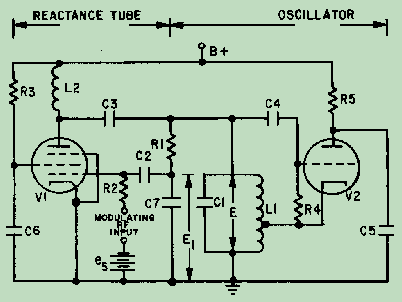
METHODS OF FREQUENCY MODULATION. - The circuit shown earlier in figure 2-6 and the discussion in previous paragraphs were for illustrative purposes only. In reality, such a circuit would not be practical. However, the basic principle involved (the change in reactance of an oscillator circuit in accordance with the modulating voltage) constitutes one of the methods of developing a frequency-modulated wave. Reactance-Tube Modulation. - In direct modulation, an oscillator is frequency modulated by a REACTANCE TUBE that is in parallel (SHUNT) with the oscillator tank circuit. (The terms "shunt" or "shunting" will be used in this module to mean the same as "parallel" or "to place in parallel with" components.) This is illustrated in figure 2-11. The oscillator is a conventional Hartley circuit with the reactance-tube circuit in parallel with the tank circuit of the oscillator tube. The reactance tube is an ordinary pentode. It is made to act either capacitively or inductively; that is, its grid is excited with a voltage which either leads or lags the oscillator voltage by 90 degrees. Figure 2-11. - Reactance-tube fm modulator.
When the reactance tube is connected across the tank circuit with no modulating voltage applied, it will affect the frequency of the oscillator. The voltage across the oscillator tank circuit (L1 and C1) is also in parallel with the series network of R1 and C7. This voltage causes a current flow through R1 and C7. If R1 is at least five times larger than the capacitive reactance of C7, this branch of the circuit will be essentially resistive. Voltage E1, which is across C7, will lag current by 90 degrees. E1 is applied to the control grid of reactance tube V1. This changes plate current (Ip), which essentially flows only through the LC tank circuit. This is because the value of R1 is high compared to the impedance of the tank circuit. Since current is inversely proportional to impedance, most of the plate current coupled through C3 flows through the tank circuit. At resonance, the voltage and current in the tank circuit are in phase. Because E1 lags E by 90 degrees and I p is in phase with grid voltage E1, the superimposed current through the tank circuit lags the original tank current by 90 degrees. Both the resultant current (caused by Ip) and the tank current lag tank voltage and current by some angle depending on the relative amplitudes of the two currents. Because this resultant current is a lagging current, the impedance across the tank circuit cannot be at its maximum unless something happens within the tank to bring current and voltage into phase. Therefore, this situation continues until the frequency of oscillations in the tank circuit changes sufficiently so that the voltages across the tank and the current flowing into it are again in phase. This action is the same as would be produced by adding a reactance in parallel with the L1C1 tank. Because the superimposed current lags voltage E by 90 degrees, the introduced reactance is inductive. In NEETS, Module 2, Introduction to Alternating Current and Transformers, you learned that total inductance decreases as additional inductors are added in parallel. Because this introduced reactance effectively reduces inductance, the frequency of the oscillator increases to a new fixed value. Now let's see what happens when a modulating signal is applied. The magnitude of the introduced reactance is determined by the magnitude of the superimposed current through the tank. The magnitude of Ip for a given E1 is determined by the transconductance of V1. (Transconductance was covered in NEETS, Module 6, Introduction to Electronic Emission, Tubes, and Power Supplies.) Therefore, the value of reactance introduced into the tuned circuit varies directly with the transconductance of the reactance tube. When a modulating signal is applied to the grid of V1, both E1 and I p change, causing transconductance to vary with the modulating signal. This causes a variable reactance to be introduced into the tuned circuit. This variable reactance either adds to or subtracts from the fixed value of reactance that is introduced in the absence of the modulating signal. This action varies the reactance across the oscillator which, in turn, varies the instantaneous frequency of the oscillator. These variations in the oscillator frequency are proportional to the instantaneous amplitude of the modulating voltage. Reactance-tube modulators are usually operated at low power levels. The required output power is developed in power amplifier stages that follow the modulators. The output of a reactance-tube modulated oscillator also contains some unwanted amplitude modulation. This unwanted modulation is caused by stray capacitance and the resistive component of the RC phase splitter. The resistance is much less significant than the desired XC, but the resistance does allow some plate current to flow which is not of the proper phase relationship for good tube operation. The small amplitude modulation that this produces is easily removed by passing the oscillator output through a limiter-amplifier circuit. Semiconductor Reactance Modulator. - The SEMICONDUCTOR-REACTANCE MODULATOR is used to frequency modulate low-power semiconductor transmitters. Figure 2-12 shows a typical frequency-modulated oscillator stage operated as a reactance modulator. Q1, along with its associated circuitry, is the oscillator. Q2 is the modulator and is connected to the circuit so that its collector-to-emitter capacitance (CCE) is in parallel with a portion of the rf oscillator coil, L1. As the modulator operates, the output capacitance of Q2 is varied. Thus, the frequency of the oscillator is shifted in accordance with the modulation the same as if C1 were varied. Figure 2-12. - Reactance-semiconductor fm modulator.
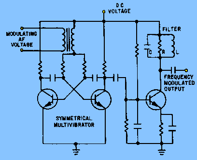
When the modulating signal is applied to the base of Q2, the emitter-to-base bias varies at the modulation rate. This causes the collector voltage of Q2 to vary at the same modulating rate. When the collector voltage increases, output capacitance CCE decreases; when the collector voltage decreases, CCE increases. An increase in collector voltage has the effect of spreading the plates of CCE farther apart by increasing the width of the barrier. A decrease of collector voltage reduces the width of the pn junction and has the same effect as pushing the capacitor plates together to provide more capacitance. When the output capacitance decreases, the instantaneous frequency of the oscillator tank circuit increases (acts the same as if C1 were decreased). When the output capacitance increases, the instantaneous frequency of the oscillator tank circuit decreases. This decrease in frequency produces a lower frequency in the output because of the shunting effect of CCE. Thus, the frequency of the oscillator tank circuit increases and decreases at an audio frequency (af) modulating rate. The output of the oscillator, therefore, is a frequency modulated rf signal. Since the audio modulation causes the collector voltage to increase and decrease, an AM component is induced into the output. This produces both an fm and AM output. The amplitude variations are then removed by placing a limiter stage after the reactance modulator and only the frequency modulation remains. Frequency multipliers or mixers (discussed in chapter 1) are used to increase the oscillator frequency to the desired output frequency. For high-power applications, linear rf amplifiers are used to increase the steady-amplitude signal to a higher power output. With the initial modulation occurring at low levels, fm represents a savings of power when compared to conventional AM. This is because fm noise-reducing properties provide a better signal-to-noise ratio than is possible with AM. Multivibrator Modulator. - Another type of frequency modulator is the astable multivibrator illustrated in figure 2-13. Inserting the modulating af voltage in series with the base-return of the multivibrator transistors causes the gate length, and thus the fundamental frequency of the multivibrator, to vary. The amount of variation will be in accordance with the amplitude of the modulating voltage. One requirement of this method is that the fundamental frequency of the multivibrator be high in relation to the highest modulating frequencies. A factor of at least 100 provides the best results. Figure 2-13. - Astable multivibrator and filter circuit for generating an fm carrier.
Recall that a multivibrator output consists of the fundamental frequency and all of its harmonics. Unwanted even harmonics are eliminated by using a SYMMETRICAL MULTIVIBRATOR circuit, as shown in figure 2-13. The desired fundamental frequency, or desired odd harmonics, can be amplified after all other odd harmonics are eliminated in the LCR filter section of figure 2-13. A single frequency-modulated carrier is then made available for further amplification and transmission. Proper design of the multivibrator will cause the frequency deviation of the carrier to faithfully follow (referred to as a "linear" function) the modulating voltage. This is true up to frequency deviations which are considerable fractions of the fundamental frequency of the multivibrator. The principal design consideration is that the RC coupling from one multivibrator transistor base to the collector of the other has a time constant which is greater than the actual gate length by a factor of 10 or more. Under these conditions, a rise in base voltage in each transistor is essentially linear from cutoff to the bias at which the transistor is switched on. Since this rise in base voltage is a linear function of time, the gate length will change as an inverse function of the modulating voltage. This action will cause the frequency to change as a linear function of the modulating voltage. The multivibrator frequency modulator has the advantage over the reactance-type modulator of a greater linear frequency deviation from a given carrier frequency. However, multivibrators are limited to frequencies below about 1 megahertz. Both systems are subject to drift of the carrier frequency and must, therefore, be stabilized. Stabilization may be accomplished by modulating at a relatively low frequency and translating by heterodyne action to the desired output frequency, as shown in figure 2-14. A 1-megahertz signal is heterodyned with 49 megahertz from the crystal-controlled oscillator to provide a stable 50-megahertz output from the mixer. If a suitably stable heterodyning oscillator is used, the frequency stability can be greatly improved. For instance, at the frequencies shown in figure 2-14, the stability of the unmodulated 50-megahertz carrier would be 50 times better than that which harmonic multiplication could provide. Figure 2-14. - Method for improving frequency stability of fm system.
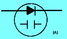
Varactor FM Modulator. - Another fm modulator which is widely used in transistorized circuitry uses a voltage-variable capacitor (VARACTOR). The varactor is simply a diode, or pn junction, that is designed to have a certain amount of capacitance between junctions. View (A) of figure 2-15 shows the varactor schematic symbol. A diagram of a varactor in a simple oscillator circuit is shown in view (B). This is not a working circuit, but merely a simplified illustration. The capacitance of a varactor, as with regular capacitors, is determined by the area of the capacitor plates and the distance between the plates. The depletion region in the varactor is the dielectric and is located between the p and n elements, which serve as the plates. Capacitance is varied in the varactor by varying the reverse bias which controls the thickness of the depletion region. The varactor is so designed that the change in capacitance is linear with the change in the applied voltage. This is a special design characteristic of the varactor diode. The varactor must not be forward biased because it cannot tolerate much current flow. Proper circuit design prevents the application of forward bias. Figure 2-15A. - Varactor symbol and schematic. SCHEMATIC SYMBOL
Figure 2-15B. - Varactor symbol and schematic. SIMPLIFIED CIRCUIT
Notice the simplicity of operation of the circuit in figure 2-16. An af signal that is applied to the input results in the following actions: (1) On the positive alternation, reverse bias increases and the dielectric (depletion region) width increases. This decreases capacitance which increases the frequency of the oscillator. (2) On the negative alternation, the reverse bias decreases, which results in a decrease in oscillator frequency. Figure 2-16. - Varactor fm modulator.
Many different fm modulators are available, but they all use the basic principles you have just studied. The main point to remember is that an oscillator must be used to establish the reference (carrier) frequency. Secondly, some method is needed to cause the oscillator to change frequency in accordance with an af signal. Anytime this can be accomplished, we have a frequency modulator. Q.7 How does the reactance-tube modulator impress intelligence onto an rf carrier? |
|
|
|
Integrated Publishing, Inc. - A (SDVOSB) Service Disabled Veteran Owned Small Business
|