Custom Search
|
|
  |
|
|
Bulk-Effect Semiconductors BULK-EFFECT SEMICONDUCTORS are unlike normal pn-junction diodes in both construction and operation. Some types have no junctions and the processes necessary for operation occur in a solid block of semiconductor material. Other types have more than one junction but still use bulk-effect action. Bulk-effect devices are among the latest of developments in the field of microwave semiconductors and new applications are being developed rapidly. They seem destined to revolutionize the field of high-power, solid-state microwave generation because they can produce much larger microwave power outputs than any currently available pn-junction semiconductors. Bulk-effect semiconductors are of two basic types: the transferred-electron devices and the avalanche transit-time devices. TRANSFERRED-ELECTRON SEMICONDUCTORS. - The discovery that microwaves could be generated by applying a steady voltage across a chip of n-type gallium-arsenide (GaAs) crystal was made in 1963 by J.B. Gunn. The device is operated by raising electrons in the crystal to conduction-band energy levels that are higher than the level they normally occupy. The overall effect is called the transferred-electron effect. In a gallium-arsenide semiconductor, empty electron conduction bands exist that are at a higher energy level than the conduction bands occupied by most of the electrons. Any electrons that do occupy the higher conduction band essentially have no mobility. If an electric field of sufficient intensity is applied to the semiconductor electrons, they will move from the low-energy conduction band to the high-energy conduction band and become essentially immobile. The immobile electrons no longer contribute to the current flow and the applied voltage progressively increases the rate at which the electrons move from the low band to the high band. As the curve in figure 2-48 shows, the maximum current rate is reached and begins to decrease even though the applied voltage continues to increase. The point at which the current on the curve begins to decrease is called the THRESHOLD. This point is the beginning of the negative-resistance region. Negative resistance is caused by electrons moving to the higher conduction band and becoming immobile. Figure 2-48. - Characteristic curve for a bulk-effect semiconductor.
If an increase in voltage is applied to a gallium-arsenide semiconductor, which is biased to operate in the negative-resistance region, it divides into regions of varying electric fields. A tiny region, known as a DOMAIN, forms that has an electric field of much greater intensity than the fields in the rest of the semiconductor. The applied voltage causes the domain to travel across the semiconductor chip from the cathode to the anode. The high field intensity of the domain is caused by the interaction of the slow electrons in the high-energy band and the faster electrons in the low-energy band. The electrons in the low-energy band travel faster than the moving domain and continually catch up during the transit from cathode to anode. When the fast electrons catch up to the domain, the high field intensity forces them into the higher band where they lose most of their mobility. This also causes them to fall behind the moving domain. Random scattering causes the electrons to lose some energy and drop back into the lower, faster, energy band and race again after the moving domain. The movement from the low-energy band to the high-energy band causes the electrons to bunch up at the back of the domain and to provide the electron-transfer energy that creates the high field intensity in the domain. The domains form at or near the cathode and move across the semiconductor to the anode, as shown in figure 2-49. As the domain disappears at the anode, a new domain forms near the cathode and repeats the process. Figure 2-49. - Gallium-arsenide semiconductor domain movement.
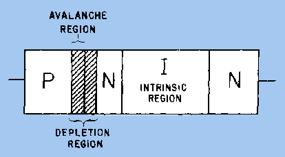
The GUNN OSCILLATOR is a source of microwave energy that uses the bulk-effect, gallium-arsenide semiconductor. The basic frequency of a gunn oscillator is inversely proportional to the transit time of a domain across the semiconductor. The transit time is proportional to the length of semiconductor material, and to some extent, the voltage applied. Each domain causes a pulse of current at the output; thus, the output is a frequency determined by the physical length of the semiconductor chip. The gunn oscillator can deliver continuous power up to about 65 milliwatts and pulsed outputs of up to about 200 watts peak. The power output of a solid chip is limited by the difficulty of removing heat from the small chip. Much higher power outputs have been achieved using wafers of gallium-arsenide as a single source. AVALANCHE TRANSIT-TIME DIODES. - Avalanche transit-time diodes, also called IMPATT (Impact Avalanche and Transit-Time) diodes, are multilayer diodes of several different types used to generate microwave power. The earliest of the avalanche transit-time diodes consists of four layers in a pnin arrangement.The intrinsic (i) layer has neither p nor n properties. The pn junction for the pnin diode, shown in figure 2-50, is strongly reverse biased to cause an avalanche in its depletion layer when the positive half cycle of a microwave signal is applied. The avalanche effect causes the electrons in the n region, which is very thin, to cross over to the intrinsic layer. The intrinsic layer is constructed so that the drift transit time causes the current to lag the signal voltage by more than 90 degrees at the desired frequency. Such a lag represents a negative resistance at the desired frequency. The pnin avalanche transit-time diode, when inserted in a microwave cavity with the proper dc bias, amplifies microwave signals introduced to the cavity. Figure 2-50. - Avalanche transit time for a pnin diode.
More recent research has shown that pin-junction diodes and simple pn-junction diodes can show negative resistance and amplification at microwave frequencies when they are reverse biased into an avalanche condition. The negative resistance in a simple pn-junction or pin diode is the result of a more complicated internal mechanism than in the pnin diode. The avalanche region and the drift region of the pnin diode are physically separate. Diodes of the pn and pin type must use the same physical region for both avalanche and drift-time control. In all types of avalanche transit-time diodes, the negative-resistance property causes dc bias energy to be absorbed by electrons in the avalanche process and given up to the applied microwave field. Q.62 What is the output frequency of an upper-sideband parametric-frequency converter? |
|
|
|
Integrated Publishing, Inc. - A (SDVOSB) Service Disabled Veteran Owned Small Business
|