Custom Search
|
|
  |
|
|
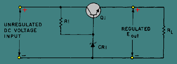
The schematic for a typical series voltage regulator is shown in figure 4-34. Notice that this regulator has a transistor (Q1) in the place of the variable resistor found in figure 4-32. Because the total load current passes through this transistor, it is sometimes called a "pass transistor." Other components which make up the circuit are the current limiting resistor (R1) and the Zener diode (CR1). Figure 4-34. - Series voltage regulator.
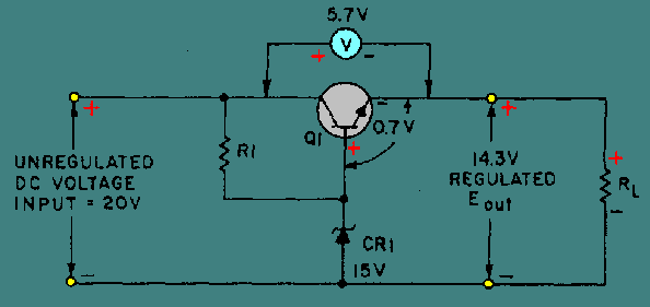
Recall that a Zener diode is a diode that block current until a specified voltage is applied. Remember also that the applied voltage is called the breakdown, or Zener voltage. Zener diodes are available with different Zener voltages. When the Zener voltage is reached, the Zener diode conducts from its anode to its cathode (with the direction of the arrow). In this voltage regulator, Q1 has a constant voltage applied to its base. This voltage is often called the reference voltage. As changes in the circuit output voltage occur, they are sensed at the emitter of Q1 producing a corresponding change in the forward bias of the transistor. In other words, Q1 compensates by increasing or decreasing its resistance in order to change the circuit voltage division. Now, study figure 4-35. Voltages are shown to help you understand how the regulator operates. The Zener used in this regulator is a 15-volt Zener. In this instance the Zener or breakdown voltage is 15 volts. The Zener establishes the value of the base voltage for Q1. The output voltage will equal the Zener voltage minus a 0.7-volt drop across the forward biased base-emitter junction of Q1, or 14.3 volts. Because the output voltage is 14.3 volts, the voltage drop across Q1 must be 5.7 volts. Figure 4-35. - Series voltage regulator (with voltages).
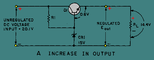
Study figure 4-36, view A, in order to understand what happens when the input voltage exceeds 20 volts. Notice the input and output voltages of 20.1 and 14.4 volts, respectively. The 14.4 output voltage is a momentary deviation, or variation, from the required regulated output voltage of 14.3 and is the result of a rise in the input voltage to 20.1 volts. Since the base voltage of Q1 is held at 15 volts by CR1, the forward bias of Q1 changes to 0.6 volt. Because this bias voltage is less than the normal 0.7 volt, the resistance of Q1 increases, thereby increasing the voltage drop across the transistor to 5.8 volts. This voltage drop restores the output voltage to 14.3 volts. The entire cycle takes only a fraction of a second and, therefore, the change is not visible on an oscilloscope or readily measurable with other standard test equipment. Figure 4-36A. - Series voltage regulator. INCREASE IN OUTPUT
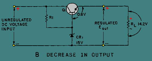
View B is a schematic diagram for the same series voltage regulator with one significant difference. The output voltage is shown as 14.2 volts instead of the desired 14.3 volts. In this case, the load has increased causing a lowered voltage drop across RL to 14.2 volts. When the output decreases, the forward bias of Q1 increases to 0.8 volt because Zener diode CR1 maintains the base voltage of Q1 at 15 volts. This 0.8 volt is the difference between the Zener reference voltage of 15 volts and the momentary output voltage. (15 V - 14.2 V = 0.8 V). At this point, the larger forward bias on Q1 causes the resistance of Q1 to decrease, thereby causing the voltage drop across Q1 to return to 5.7 volts. This then causes the output voltage to return to 14.3 volts. Figure 4-36B. - Series voltage regulator. DECREASE IN OUTPUT
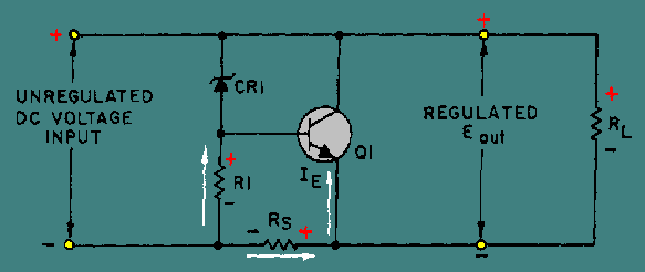
The schematic shown in figure 4-37 is that of a shunt voltage regulator. Notice that Q1 is in parallel with the load. Components of this circuit are identical with those of the series voltage regulator except for the addition of fixed resistor RS. As you study the schematic, you will see that this resistor is connected in series with the output load resistance. The current limiting resistor (R1) and Zener diode (CR1) provide a constant reference voltage for the base-collector junction of Q1. Notice that the bias of Q1 is determined by the voltage drop across RS and R1. As you should know, the amount of forward bias across a transistor affects its total resistance. In this case, the voltage drop across RS is the key to the total circuit operation. Figure 4-37. - Shunt voltage regulator.
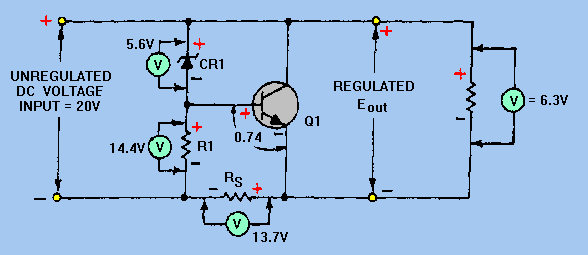
Figure 4-38 is the schematic for a typical shunt-type regulator. Notice that the schematic is identical to the schematic shown in figure 4-37 except that voltages are shown to help you understand the functions of the various components. In the circuit shown, the voltage drop across the Zener diode (CR1) remains constant at 5.6 volts. This means that with a 20-volt input voltage, the voltage drop across R1 is 14.4 volts. With a base-emitter voltage of 0.7 volt, the output voltage is equal to the sum of the voltages across CR1 and the voltage at the base-emitter junction of Q1. In this example, with an output voltage of 6.3 volts and a 20-volt input voltage, the voltage drop across RS equals 13.7 volts. Study the schematic to understand fully how these voltages are developed. Pay close attention to the voltages shown. Figure 4-38. - Shunt voltage regulator (with voltages).
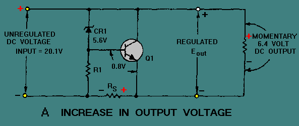
Now, refer to view A of figure 4-39. This figure shows the schematic diagram of the same shunt voltage regulator as that shown in figure 4-38 with an increased input voltage of 20.1 volts. This increases the forward bias on Q1 to 0.8 volt. Recall that the voltage drop across CR1 remains constant at 5.6 volts. Since the output voltage is composed of the Zener voltage and the base-emitter voltage, the output voltage momentarily increases to 6.4 volts. At this time, the increase in the forward bias of Q1 lowers the resistance of the transistor allowing more current to flow through it. Since this current must also pass through RS, there is also an increase in the voltage drop across this resistor. The voltage drop across RS is now 13.8 volts and therefore the output voltage is reduced to 6.3 volts. Remember, this change takes place in a fraction of a second. Figure 4-39A. - Shunt voltage regulator. INCREASE IN OUTPUT VOLTAGE
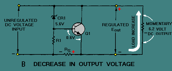
Study the schematic shown in view B. Although this schematic is identical to the other shunt voltage schematics previously illustrated and discussed, the output voltage is different. The load current has increased causing a momentary drop in voltage output to 6.2 volts. Recall that the circuit was designed to ensure a constant output voltage of 6.3 volts. Since the output voltage is less than that required, changes occur in the regulator to restore the output to 6.3 volts. Because of the 0.1 volt drop in the output voltage, the forward bias of Q1 is now 0.6 volt. This decrease in the forward bias increases the resistance of the transistor, thereby reducing the current flow through Q1 by the same amount that the load current increased. The current flow through RS returns to its normal value and restores the output voltage to 6.3 volts. Figure 4-39B. - Shunt voltage regulator. DECREASE IN OUTPUT VOLTAGE
Q.33 In figure 4-37, the voltage drop across RS and R1 determines the amount
of base-emitter ____ for Q1. |
 |