Custom Search
|
|
  |
|
|
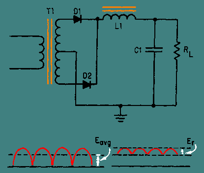
LC Choke-Input Filter The LC choke-input filter is used primarily in power supplies where voltage regulation is important and where the output current is relatively high and subject to varying load conditions. This filter is used in high power applications such as those found in radars and communication transmitters. Notice in figure 4-19 that this filter consists of an input inductor (L1), or filter choke, and an output filter capacitor (C1). Inductor L1 is placed at the input to the filter and is in series with the output of the rectifier circuit. Since the action of an inductor is to oppose any change in current flow, the inductor tends to keep a constant current flowing to the load throughout the complete cycle of the applied voltage. As a result, the output voltage never reaches the peak value of the applied voltage. Instead, the output voltage approximates the average value of the rectified input to the filter, as shown in the figure. The reactance of the inductor (XL) reduces the amplitude of ripple voltage without reducing the dc output voltage by an appreciable amount. (The dc resistance of the inductor is just a few ohms.) Figure 4-19. - LC choke-input filter.
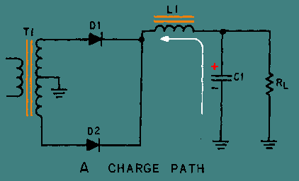
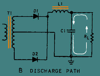
The shunt capacitor (C1) charges and discharges at the ripple frequency rate, but the amplitude of the ripple voltage (Er) is relatively small because the inductor (L1) tends to keep a constant current flowing from the rectifier circuit to the load. In addition, the reactance of the shunt capacitor (XC) presents a low impedance to the ripple component existing at the output of the filter, and thus shunts the ripple component around the load. The capacitor attempts to hold the output voltage relatively constant at the average value of the voltage. The value of the filter capacitor (C1) must be relatively large to present a low opposition (XC) to the pulsating current and to store a substantial charge. The rate of the charge for the capacitor is limited by the low impedance of the ac source (the transformer), by the small resistance of the diode, and by the counter electromotive force (CEMF) developed by the coil. Therefore, the RC charge time constant is short compared to its discharge time. (This comparison in RC charge and discharge paths is illustrated in views A and B of figure 4-20.) Consequently, when the pulsating voltage is first applied to the LC choke-input filter, the inductor (L1) produces a CEMF which opposes the constantly increasing input voltage. The net result is to effectively prevent the rapid charging of the filter capacitor (C1). Thus, instead of reaching the peak value of the input voltage, C1 only charges to the average value of the input voltage. After the input voltage reaches its peak and decreases sufficiently, the capacitor C1) attempts to discharge through the load resistance RL). C1 will only partially discharge, as indicated in view B of the figure, because of its relatively long discharge time constant. The larger the value of the filter capacitor, the better the filtering action. However, because of physical size, there is a practical limitation to the maximum value of the capacitor. Figure 4-20A. - LC choke-input filter (charge and discharge paths). CHARGE PATH
Figure 4-20B. - LC choke-input filter (charge and discharge paths). DISCHARGE PATH
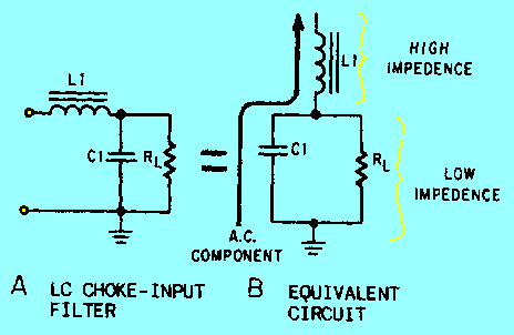
The inductor (also referred to as the filter choke or coil) serves to maintain the current flow to the filter output (RL) at a nearly constant level during the charge and discharge periods of the filter capacitor. The inductor (L1) and the capacitor (C1) form a voltage divider for the ac component (ripple) of the applied input voltage. This is shown in views A and B of figure 4-21. As far as the ripple component is concerned, the inductor offers a high impedance (Z) and the capacitor offers a low impedance (view B). As a result, the ripple component (Er) appearing across the load resistance is greatly attenuated (reduced). The inductance of the filter choke opposes changes in the value of the current flowing through it; therefore, the average value of the voltage produced across the capacitor contains a much smaller value of ripple component (Er) than the value of ripple produced across the choke. Figure 4-21. - LC choke-input filter.
Now look at figure 4-22 which illustrates a complete cycle of operation for a full-wave rectifier circuit used to supply the input voltage to the filter. The rectifier voltage is developed across the capacitor (C1). The ripple voltage at the output of the filter is the alternating component of the input voltage reduced in amplitude by the filter section. Each time the anode of a diode goes positive with respect to the cathode, the diode conducts and C1 charges. Conduction occurs twice during each cycle for a full-wave rectifier. For a 60-hertz supply, this produces a 120-hertz ripple voltage. Although the diodes alternate (one conducts while the other is nonconducting), the filter input voltage is not steady. As the anode voltage of the conducting diode increases (on the positive half of the cycle), capacitor C1 charges-the charge being limited by the impedance of the secondary transformer winding, the diode's forward (cathode-to-anode) resistance, and the counter electromotive force developed by the choke. During the nonconducting interval (when the anode voltage drops below the capacitor charge voltage), C1 discharges through the load resistor (RL). The components in the discharge path have a long time constant; thus, C1 discharges more slowly than it charges. Figure 4-22. - Filtering action of the LC choke-input filter.
The choke (L1) is usually a large value, from 1 to 20 henries, and offers a large inductive reactance to the 120-hertz ripple component produced by the rectifier. Therefore, the effect that L1 has on the charging of the capacitor (C1) must be considered. Since L1 is connected in series with the parallel branch consisting of C1 and RL, a division of the ripple (ac) voltage and the output (dc) voltage occurs. The greater the impedance of the choke, the less the ripple voltage that appears across C1 and the output. The dc output voltage is fixed mainly by the dc resistance of the choke. Now that you have read how the LC choke-input filter functions, it will be discussed with actual component values applied. For simplicity, the input frequency at the primary of the transformer will be 117 volts 60 hertz. Both half-wave and full-wave rectifier circuits will be used to provide the input to the filter. Starting with the half-wave configuration shown in figure 4-23 , the basic parameters are: With 117 volts ac rms applied to the T1 primary, 165 volts ac peak is available at the secondary [(117 V) X (1.414) = 165 V]. You should recall that the ripple frequency of this half-wave rectifier is 60 hertz. Therefore, the capacitive reactance of C1 is:
Figure 4-23. - Half-wave rectifier with an LC choke-input filter.
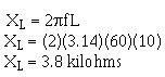
This means that the capacitor (C1) offers 265 ohms of opposition to the ripple current. Note, however, that the capacitor offers an infinite impedance to direct current. The inductive reactance of L1 is:
The above calculation shows that L1 offers a relatively high opposition (3.8 kilohms) to the ripple in comparison to the opposition offered by C1 (265 ohms). Thus, more ripple voltage will be dropped across L1 than across C1. In addition, the impedance of C1 (265 ohms) is relatively low with respect to the resistance of the load (10 kilohms). Therefore, more ripple current flows through C1 than the load. In other words, C1 shunts most of the ac component around the load. |
 |
|
|
Integrated Publishing, Inc. - A (SDVOSB) Service Disabled Veteran Owned Small Business
|