Custom Search
|
|
  |
|
|
Figure 3-50. - JFET symbols and bias voltages.
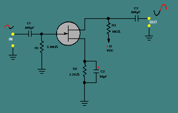
Because the materials used to make the bar and the gate are reversed, source voltage potentials must also be reversed. The P-channel JFET therefore requires a positive gate voltage to be reverse biased, and current flows through it from drain to source. Figure 3-51 shows a basic common-source amplifier circuit containing an N-channel JFET. The characteristics of this circuit include high input impedance and a high voltage gain. The function of the circuit components in this figure is very similar to those in a triode vacuum tube common-cathode amplifier circuit. C1 and C3 are the input and output coupling capacitors. R1 is the gate return resistor and functions much like the grid return resistor in a vacuum tube circuit. It prevents unwanted charge buildup on the gate by providing a discharge path for C1. R2 and C2 provide source self-bias for the JFET, which operates like cathode self-bias. R3 is the drain load resistor, which acts like the plate or collector load resistor. Figure 3-51. - JFET common source amplifier.
The phase shift of 180 degrees between input and output signals is the same as that of common-cathode vacuum tube circuits (and common-emitter transistor circuits). The reason for the phase shift can be seen easily by observing the operation of the N-channel JFET. On the positive alternation of the input signal, the amount of reverse bias on the P-type gate material is reduced, thus increasing the effective cross-sectional area of the channel and decreasing source-to-drain resistance. When resistance decreases, current flow through the JFET increases. This increase causes the voltage drop across R3 to increase, which in turn causes the drain voltage to decrease. On the negative alternation of the cycle, the amount of reverse bias on the gate of the JFET is increased and the action of the circuit is reversed. The result is an output signal, which is an amplified 180-degree-out-of-phase version of the input signal. A second type of field-effect transistor has been introduced in recent years that has some advantages over the JFET. This device is the metal oxide semiconductor field effect transistor (MOSFET). The MOSFET has an even higher input impedance than the JFET (10 to 100 million megohms). Therefore, the MOSFET is even less of a load on preceding circuits. The extremely high input impedance, combined with a high gain factor, makes the MOSFET a highly efficient input device for RF/IF amplifiers and mixers and for many types of test equipment. The MOSFET is normally constructed so that it operates in one of two basic modes: the depletion mode or the enhancement mode. The depletion mode MOSFET has a heavily doped channel and uses reverse bias on the gate to cause a depletion of current carriers in the channel. The JFET also operates in this manner. The enhancement mode MOSFET has a lightly doped channel and uses forward bias to enhance the current carriers in the channel. A MOSFET can be constructed that will operate in either mode depending upon what type of bias is applied, thus allowing a greater range of input signals. In addition to the two basic modes of operation, the MOSFET, like the JFET, is of either the P-channel type or the N-channel type. Each type has four elements: gate, source, drain, and substrate. The schematic symbols for the four basic variations of the MOSFET are shown in views A, B, C, and D of figure 3-52. Figure 3-52A. - MOSFET symbols.
Figure 3-52B. - MOSFET symbols.
Figure 3-52C. - MOSFET symbols.
Figure 3-52D. - MOSFET symbols.
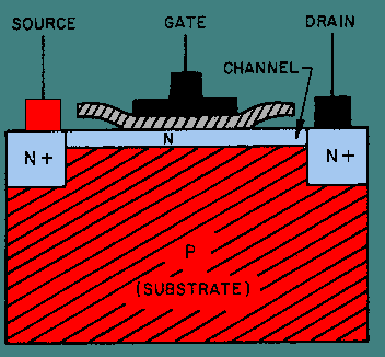
The construction of an N-channel MOSFET is shown in figure 3-53. Heavily doped N-type regions (indicated by the N+) are diffused into a P-type substrate or base. A channel of regular N-type material is diffused between the heavily doped N-type regions. A metal oxide insulating layer is then formed over the channel, and a metal gate layer is deposited over the insulating layer. There is no electrical connection between the gate and the rest of the device. This construction method results in the extremely high input impedance of the MOSFET. Another common name for the device, derived from the construction method, is the insulated gate field effect transistor (IGFET). Figure 3-53. - MOSFET structure.
The operation of the MOSFET, or IGFET, is basically the same as the operation of the JFET. The current flow between the source and drain can be controlled by using either of two methods or by using a combination of the two methods. In one method the drain voltage controls the current when the gate potential is at zero volts. A voltage is applied to the gate in the second method. An electric field is formed by the gate voltage that affects the current flow in the channel by either depleting or enhancing the number of current carriers available. As previously stated, a reverse bias applied to the gate depletes the carriers, and a forward bias enhances the carriers. The polarity of the voltages required to forward or reverse bias a MOSFET depends upon whether it is of the P-channel type or the N-channel type. The effects of reverse-bias voltage on a MOSFET designed to operate in the depletion mode are illustrated in views A, B, and C of figure 3-54. The amount of reverse bias applied has a direct effect on the width of the current channel and, thus, the amount of drain current (ID). |
 |
|
|
Integrated Publishing, Inc. - A (SDVOSB) Service Disabled Veteran Owned Small Business
|