Custom Search
|
|
  |
|
|
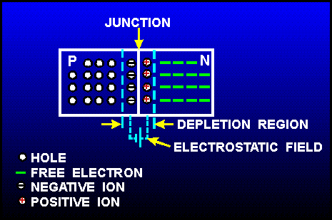
Junction Barrier Although the N-type material has an excess of free electrons, it is still electrically neutral. This is because the donor atoms in the N material were left with positive charges after free electrons became available by covalent bonding (the protons outnumbered the electrons). Therefore, for every free electron in the N material, there is a corresponding positively charge atom to balance it. The end result is that the N material has an overall charge of zero. By the same reasoning, the P-type material is also electrically neutral because the excess of holes in this material is exactly balanced by the number of electrons. Keep in mind that the holes and electrons are still free to move in the material because they are only loosely bound to their parent atoms. It would seem that if we joined the N and P materials together by one of the processes mentioned earlier, all the holes and electrons would pair up. On the contrary, this does not happen. Instead the electrons in the N material diffuse (move or spread out) across the junction into the P material and fill some of the holes. At the same time, the holes in the P material diffuse across the junction into the N material and are filled by N material electrons. This process, called JUNCTION RECOMBINATION, reduces the number of free electrons and holes in the vicinity of the junction. Because there is a depletion, or lack of free electrons and holes in this area, it is known as the DEPLETION REGION. The loss of an electron from the N-type material created a positive ion in the N material, while the loss of a hole from the P material created a negative ion in that material. These ions are fixed in place in the crystal lattice structure and cannot move. Thus, they make up a layer of fixed charges on the two sides of the junction as shown in figure 1-17. On the N side of the junction, there is a layer of positively charged ions; on the P side of the junction, there is a layer of negatively charged ions. An electrostatic field, represented by a small battery in the figure, is established across the junction between the oppositely charged ions. The diffusion of electrons and holes across the junction will continue until the magnitude of the electrostatic field is increased to the point where the electrons and holes no longer have enough energy to overcome it, and are repelled by the negative and positive ions respectively. At this point equilibrium is established and, for all practical purposes, the movement of carriers across the junction ceases. For this reason, the electrostatic field created by the positive and negative ions in the depletion region is called a barrier. Figure 1-17. - The PN junction barrier formation.
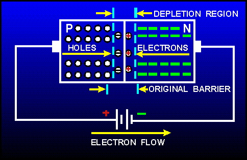
The action just described occurs almost instantly when the junction is formed. Only the carriers in the immediate vicinity of the junction are affected. The carriers throughout the remainder of the N and P material are relatively undisturbed and remain in a balanced condition. FORWARD BIAS. - An external voltage applied to a PN junction is call BIAS. If, for example, a battery is used to supply bias to a PN junction and is connected so that its voltage opposes the junction field, it will reduce the junction barrier and, therefore, aid current flow through the junction. This type of bias is known as forward bias, and it causes the junction to offer only minimum resistance to the flow of current. Forward bias is illustrated in figure 1-18. Notice the positive terminal of the bias battery is connected to the P-type material and the negative terminal of the battery is connected to the N-type material. The positive potential repels holes toward the junction where they neutralize some of the negative ions. At the same time the negative potential repels electrons toward the junction where they neutralize some of the positive ions. Since ions on both sides of the barrier are being neutralized, the width of the barrier decreases. Thus, the effect of the battery voltage in the forward-bias direction is to reduce the barrier potential across the junction and to allow majority carriers to cross the junction. Current flow in the forward-biased PN junction is relatively simple. An electron leaves the negative terminal of the battery and moves to the terminal of the N-type material. It enters the N material, where it is the majority carrier and moves to the edge of the junction barrier. Because of forward bias, the barrier offers less opposition to the electron and it will pass through the depletion region into the P-type material. The electron loses energy in overcoming the opposition of the junction barrier, and upon entering the P material, combines with a hole. The hole was produced when an electron was extracted from the P material by the positive potential of the battery. The created hole moves through the P material toward the junction where it combines with an electron. Figure 1-18. - Forward-biased PN junction.
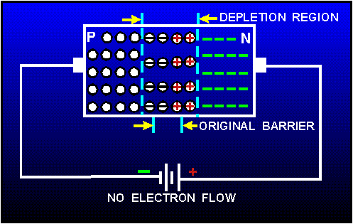
It is important to remember that in the forward biased condition, conduction is by MAJORITY current carriers (holes in the P-type material and electrons in the N-type material). Increasing the battery voltage will increase the number of majority carriers arriving at the junction and will therefore increase the current flow. If the battery voltage is increased to the point where the barrier is greatly reduced, a heavy current will flow and the junction may be damaged from the resulting heat. REVERSE BIAS. - If the battery mentioned earlier is connected across the junction so that its voltage aids the junction, it will increase the junction barrier and thereby offer a high resistance to the current flow through the junction. This type of bias is known as reverse bias. To reverse bias a junction diode, the negative battery terminal is connected to the P-type material, and the positive battery terminal to the N-type material as shown in figure 1-19. The negative potential attracts the holes away from the edge of the junction barrier on the P side, while the positive potential attracts the electrons away from the edge of the barrier on the N side. This action increases the barrier width because there are more negative ions on the P side of the junction, and more positive ions on the N side of the junction. Notice in the figure the width of the barrier has increased. This increase in the number of ions prevents current flow across the junction by majority carriers. However, the current flow across the barrier is not quite zero because of the minority carriers crossing the junction. As you recall, when the crystal is subjected to an external source of energy (light, heat, etc.), electron-hole pairs are generated. The electron-hole pairs produce minority current carriers. There are minority current carriers in both regions: holes in the N material and electrons in the P material. With reverse bias, the electrons in the P-type material are repelled toward the junction by the negative terminal of the battery. As the electron moves across the junction, it will neutralize a positive ion in the N-type material. Similarly, the holes in the N-type material will be repelled by the positive terminal of the battery toward the junction. As the hole crosses the junction, it will neutralize a negative ion in the P-type material. This movement of minority carriers is called MINORITY CURRENT FLOW, because the holes and electrons involved come from the electron-hole pairs that are generated in the crystal lattice structure, and not from the addition of impurity atoms. Figure 1-19. - Reverse-biased PN junction.
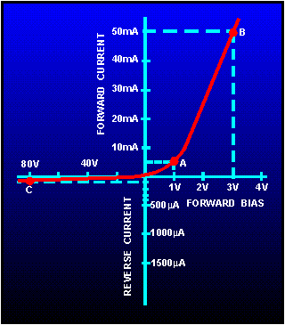
Therefore, when a PN junction is reverse biased, there will be no current flow because of majority carriers but a very small amount of current because of minority carriers crossing the junction. However, at normal operating temperatures, this small current may be neglected. In summary, the most important point to remember about the PN junction diode is its ability to offer very little resistance to current flow in the forward-bias direction but maximum resistance to current flow when reverse biased. A good way of illustrating this point is by plotting a graph of the applied voltage versus the measured current. Figure 1-20 shows a plot of this voltage-current relationship (characteristic curve) for a typical PN junction diode. Figure 1-20. - PN junction diode characteristic curve.
To determine the resistance from the curve in this figure we can use Ohm's law:
For example at point A the forward-bias voltage is 1 volt and the forward-bias current is 5 milliamperes. This represents 200 ohms of resistance (1 volt/5mA = 200 ohms). However, at point B the voltage is 3 volts and the current is 50 milliamperes. This results in 60 ohms of resistance for the diode. Notice that when the forward-bias voltage was tripled (1 volt to 3 volts), the current increased 10 times (5mA to 50 mA). At the same time the forward-bias voltage increased, the resistance decreased from 200 ohms to 60 ohms. In other words, when forward bias increases, the junction barrier gets smaller and its resistance to current flow decreases. On the other hand, the diode conducts very little when reverse biased. Notice at point C the reverse bias voltage is 80 volts and the current is only 100 microamperes. This results in 800 k ohms of resistance, which is considerably larger than the resistance of the junction with forward bias. Because of these unusual features, the PN junction diode is often used to convert alternating current into direct current (rectification). Q.24 What is the name of the area in a PN junction that has a shortage of electrons and
holes? |
 |
|
|
Integrated Publishing, Inc. - A (SDVOSB) Service Disabled Veteran Owned Small Business
|