Custom Search
|
|
  |
|
|
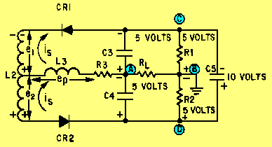
RATIO DETECTOR The RATIO DETECTOR uses a double-tuned transformer to convert the instantaneous frequency variations of the fm input signal to instantaneous amplitude variations. These amplitude variations are then rectified to provide a dc output voltage which varies in amplitude and polarity with the input signal frequency. This detector demodulates fm signals and suppresses amplitude noise without the need of limiter stages. Circuit Operation Figure 3-12 shows a typical ratio detector. The input tank capacitor (C1) and the primary of transformer T1 (L1) are tuned to the center frequency of the fm signal to be demodulated. The secondary winding of T1 (L2) and capacitor C2 also form a tank circuit tuned to the center frequency. Tertiary (third) winding L3 provides additional inductive coupling which reduces the loading effect of the secondary on the primary circuit. Diodes CR1 and CR2 rectify the signal from the secondary tank. Capacitor C5 and resistors R1 and R2 set the operating level of the detector. Capacitors C3 and C4 determine the amplitude and polarity of the output. Resistor R3 limits the peak diode current and furnishes a dc return path for the rectified signal. The output of the detector is taken from the common connection between C3 and C4. Resistor RL is the load resistor. R5, C6, and C7 form a low-pass filter to the output. Figure 3-12. - Ratio detector.
This circuit operates on the same principles of phase shifting as did the Foster-Seeley discriminator. In that discussion, vector diagrams were used to illustrate the voltage amplitudes and polarities for conditions at resonance, above resonance, and below resonance. The same vector diagrams apply to the ratio detector but will not be discussed here. Instead, you will study the resulting current flows and polarities on simplified schematic diagrams of the detector circuit. OPERATION AT RESONANCE. - When the input voltage ep is applied to the primary in figure 3-12 it also appears across L3 because, by inductive coupling, it is effectively connected in parallel with the primary tank circuit. At the same time, a voltage is induced in the secondary winding and causes current to flow around the secondary tank circuit. At resonance the tank acts like a resistive circuit; that is, the tank current is in phase with the primary voltage ep. The current flowing in the tank circuit causes voltages e1 and e2 to be developed in the secondary winding of T1. These voltages are of equal magnitude and of opposite polarity with respect to the center tap of the winding. Since the winding is inductive, the voltage drop across it is 90 degrees out of phase with the current through it. Figure 3-13 is a simplified schematic diagram of a ratio detector at resonance. The voltage applied to the cathode of CR1 is the vector sum of e1 and ep. Likewise, the voltage applied to the anode of CR2 is the vector sum of e2 and ep. No phase shift occurs at resonance and both voltages are equal. Both diodes conduct equally. This equal current flow causes the same voltage drop across both R1 and R2. C3 and C4 will charge to equal voltages with opposite polarities. Let's assume that the voltages across C3 and C4 are equal in amplitude (5 volts) and of opposite polarity and the total charge across C5 is 10 volts. R1 and R2 will each have 5 volts dropped across them because they are of equal values. The output is taken between points A and B. To find the output voltage, you algebraically add the voltages between points A and B (loop ACB or ADB). Point A to point D is -5 volts. Point D to point B is + 5 volts. Their algebraic sum is 0 volts and the output voltage is 0 at resonance. If the voltages on branch ACB were figured, the same output would be found because the circuit branches are in parallel. Figure 3-13. - Current flow and polarities at resonance.
When the input signal reverses polarity, the secondary voltage across L2 also reverses. The diodes will be reverse biased and no current will flow. Meanwhile, C5 retains most of its charge because of the long time constant offered in combination with R1 and R2. This slow discharge helps to maintain the output. OPERATION ABOVE RESONANCE. - When a tuned circuit (figure 3-14) operates at a frequency higher than resonance, the tank is inductive. The secondary current i s lags the primary voltage ep. Secondary voltage e1 is nearer in phase with primary voltage e p, while e2 is shifted further out of phase with ep. The vector sum of e1 and ep is larger than that of e2 and ep. Therefore, the voltage applied to the cathode of CR1 is greater than the voltage applied to the anode of CR2 above resonance. Figure 3-14. - Current flow and polarities above resonance.
Assume that the voltages developed above resonance are such that the higher voltage on the cathode of CR1 causes C3 to charge to 8 volts. The lower voltage on the anode of CR2 causes C4 to charge to 2 volts. Capacitor C5 remains charged to the sum of these two voltages, 10 volts. Again, by adding the voltages in loop ACB or ADB between points A and B, you can find the output voltage. Point A to point D equals -2 volts. Point D to point B equals +5 volts. Their algebraic sum, and the output, equals +3 volts when tuned above resonance. During the negative half cycle of the input signal, the diodes are reverse biased and C5 helps maintain a constant output. OPERATION BELOW RESONANCE. - When a tuned circuit operates below resonance (figure 3-15),it is capacitive. Secondary current is leads the primary voltage ep and secondary voltage e2 is nearer in phase with primary voltage ep. The vector sum of e2 and ep is larger than the sum of e1 and ep. The voltage applied to the anode of CR2 becomes greater than the voltage applied to the cathode of CR1 below resonance. Figure 3-15. - Current flow and polarities below resonance.
Assume that the voltages developed below resonance are such that the higher voltage on the anode of CR2 causes C4 to charge to 8 volts. The lower voltage on the cathode of CR1 causes C3 to charge to 2 volts. Capacitor C5 remains charged to the sum of these two voltages, 10 volts. The output voltage equals -8 volts plus +5 volts, or -3 volts, when tuned below resonance. During the negative half cycle of the input signal, the diodes are reverse biased and C5 helps maintain a constant output. Advantage of a Ratio Detector The ratio detector is not affected by amplitude variations on the fm wave. The output of the detector adjusts itself automatically to the average amplitude of the input signal. C5 charges to the sum of the voltages across R1 and R2 and, because of its time constant, tends to filter out any noise impulses. Before C5 can charge or discharge to the higher or lower potential, the noise disappears. The difference in charge across C5 is so slight that it is not discernible in the output. Ratio detectors can operate with as little as 100 millivolts of input. This is much lower than that required for limiter saturation and less gain is required from preceding stages. Q.26 What is the primary advantage of a ratio detector? |
|
|
|
Integrated Publishing, Inc. - A (SDVOSB) Service Disabled Veteran Owned Small Business
|