Custom Search
|
|
  |
|
|
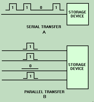
SHIFT REGISTERS A shift register is a register in which the contents may be shifted one or more places to the left or right. This type of register is capable of performing a variety of functions. It may be used for serial-to-parallel conversion and for scaling binary numbers. Before we get into the operation of the shift register, let's discuss serial-to-parallel conversion, parallel-to-serial conversion, and scaling. Serial and Parallel Transfers and Conversion Serial and parallel are terms used to describe the method in which data or information is moved from one place to another. SERIAL TRANSFER means that the data is moved along a single line one bit at a time. A control pulse is required to move each bit. PARALLEL TRANSFER means that each bit of data is moved on its own line and that all bits transfer simultaneously as they did in the parallel register. A single control pulse is required to move all bits. Figure 3-29 shows how both of these transfers occur. In each case, the four-bit word 1101 is being transferred to a storage device. In view A, the data moves along a single line. Each bit of the data will be stored by an individual control pulse. In view B, each bit has a separate input line. One control pulse will cause the entire word to be stored. Figure 3-29. - Data transfer methods: A. Serial transfer; B. Parallel transfer.
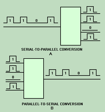
Serial-to-parallel conversion or parallel-to-serial conversion describes the manner in which data is stored in a storage device and the manner in which that data is removed from the storage device. Serial-to-parallel conversion means that data is transferred into the storage device or register in serial fashion and removed in parallel fashion, as in figure 3-30, view A. Parallel-to-serial conversion means the data is transferred into the storage device in parallel and removed as serial data, as shown in view B. Figure 3-30. - Data conversion methods: A. Serial-to-parallel; B. Parallel-to-serial.
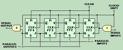
Serial transfer takes time. The longer the word length, the longer the transfer will take. Although parallel transfer is much faster, it requires more circuitry to transfer the data. Scaling SCALING means to change the magnitude of a number. Shifting binary numbers to the left increases their value, and shifting to the right decreases their value. The increase or decrease in value is based on powers of 2. A shift of one place to the left increases the value by a power of 2, which in effect is multiplying the number by 2. To demonstrate this, let's assume that the following block diagram is a 5-bit shift register containing the binary number 01100. 0 1 1 0 0 Shifting the entire number one place to the left will put the register in the following condition: 1 1 0 0 0 The binary number 01100 has a decimal equivalent of 12. If we convert 110002 to decimal, we find it has a value of 2410. By shifting the number one place to the left, we have multiplied it by 2. A shift of two places to the left would be the equivalent of multiplying the number by 22, or 4; three places by 23, or 8; and so forth. Shifting a binary number to the right decreases the value of the number by a power of 2 for each place. Let's look at the same 5-bit register containing 011002 and shift the number to the right. 0 1 1 0 0 A shift of one place to the right will result in the register being in the following condition: 0 0 1 1 0 By comparing decimal equivalents you can see that we have decreased the value from 1210 to 610. We have effectively divided the number by 2. A shift of two places to the right is the equivalent of dividing the number by 22, or 4; three places by 23; or 8; and so forth. Shift Register Operations Figure 3-31 shows a typical 4-bit shift register. This particular register is capable of left shifts only. There are provisions for serial and parallel input and serial and parallel output. Additional circuitry would be required to make right shifts possible. Figure 3-31. - Shift register.
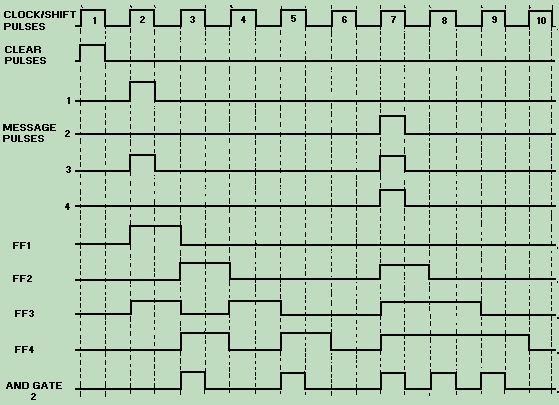
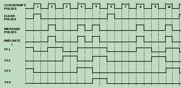
Before any operation takes place, a CLEAR pulse is applied to the RESET terminal of each FF to ensure that the Q output is LOW. The simplest modes of operation for this register are the parallel inputs and outputs. Parallel data is applied to the SET inputs of the FFs and results in either a 1 or 0 output, depending on the input. The outputs of the FFs may be sampled for parallel output. In this mode, the register functions just like the parallel register covered earlier in this section. Parallel-to-Serial Conversion Now let's look at parallel-to-serial conversion. We will use the 4-bit shift register in figure 3-31 and the timing sequence in figure 3-32 to aid you in understanding the operations. Figure 3-32. - Parallel-to-serial conversion timing diagram.
At CP1, a CLEAR pulse is applied to all the FFs, resetting the register to a count of 0. The number 01012 is applied to the parallel inputs at CP2, causing FF1 and FF3 to set. At this point, the J inputs of FF2 and FF4 are HIGH. AND gate 2 has a LOW output since the FF4 output is LOW. This LOW output represents the first digit of the number 01012 to be output in serial form. At the same time we have HIGHs on the K inputs of FF1 and FF3. (Notice the NOT symbol on FF1 at input K. With no serial input to AND gate 1, the output is LOW; therefore, the K input to FF1 is held HIGH). With these conditions CP3 causes FF1 and FF3 to reset and FF2 and FF4 to set. The HIGH output of FF4, along with CP3, causes AND gate 2 to output a HIGH. This represents the second digit of the number 01012. At CP4, FF2 and FF4 reset, and FF3 sets. FF1 remains reset because of the HIGH at the K input. The output of AND gate 2 goes LOW because the output of FF4 is LOW and the third digit of the number is output on the serial line. CP5 causes FF4 to set and FF3 to reset. CP5 and the HIGH from FF4 cause AND gate 2 to output the last digit of the number on the serial line. It took a total of four CLK pulses to input the number in parallel and output it in serial. CP6 causes FF4 to reset and effectively clears the register for the next parallel input. Between CP7 and CP10, the number 11102 is input as parallel data and output as serial data. Serial-to-Parallel Conversion Serial input is accomplished much in the same manner as serial output. Instead of shifting the data out one bit at a time, we shift the data in one bit at a time. To understand this conversion, you should again use figure 3-31 and also the timing diagram shown in figure 3-33. In this example we will convert the number 10112 from serial data to parallel data. Figure 3-33. - Serial-to-parallel conversion timing diagram.
A CLEAR pulse resets all the FFs at CP1. At CP2, the most significant bit of the data is input to AND gate 1. This HIGH along with the clock pulse causes AND gate 1 to output a HIGH. The HIGH from the AND gate and the clock pulse applied to FF1 cause the FF to set. FFs 2, 3, and 4 are held reset. At this point, the MSD of the data has been shifted into the register. The next bit of data is a 0. The output of AND gate 1 is LOW. Because of the inverter on the K input of FF1, the FF senses a HIGH at that input and resets. At the same time this is occurring, the HIGH on the J input of FF2 (from FF1) and the CLK cause FF2 to set. The two MSDs, 1 and 0, are now in the register. CP4 causes FF3 to set and FF2 to reset. FF1 is set by the CLK pulse and the third bit of the number. The register now contains 01012, as a result of shifting the first three bits of data. The remaining bit is shifted into the register by CP5. FF1 remains set, FF2 sets, FF3 resets, and FF4 sets. At this point, the serial transfer is complete. The binary word can be sampled on the parallel output lines. Once the parallel data is transferred, a CLEAR pulse resets the FFs (CP6), and the register is ready to input the next word. Scaling Operation Using the shift register shown in figure 3-31 for scaling a number is quite simple. The number to be scaled is loaded into the register either in serial or parallel form. Once the data is in the register, the scaling takes place in the same manner as that for shifting the data for serial output. A single clock pulse will cause each bit of data to shift one place to the left. Remember that each shift is the equivalent of increasing the value by a power of 2. The scaled data is read from the parallel outputs. Care must be taken not to overshift the data to the point that the MSDs are shifted out of the register. Q.54 Serial-to-parallel and parallel-to-serial conversions are accomplished by what
type of circuit? |
|