Home
Download PDF
Order CD-ROM
Order in Print
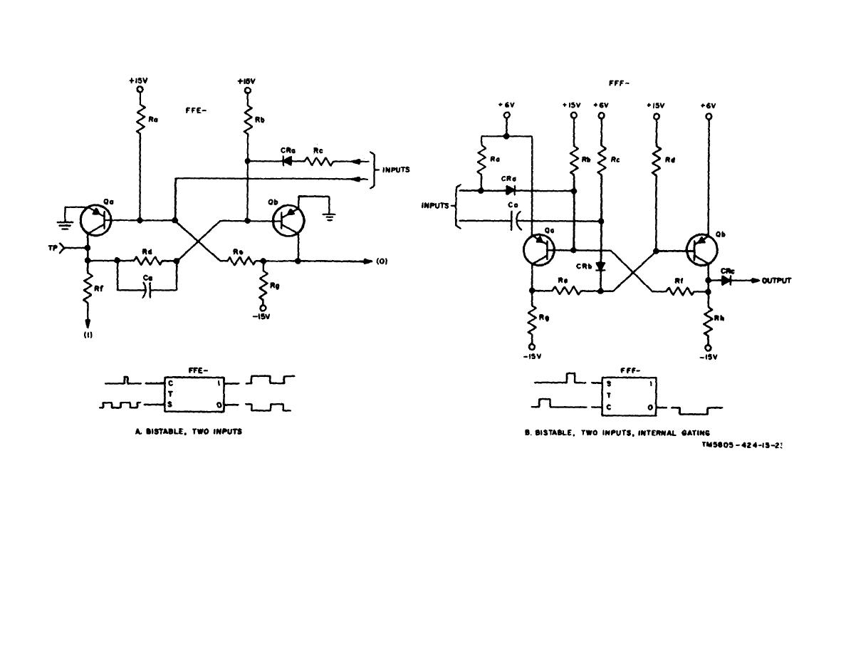
Figure 5-1. Common input bistable stages, schematic diagram and logic symbol.
Figure 5-4. Two-input bistable stage, +6-volt clamped output, schematic diagram and logic symbol
TM-11-5805-424-15 Modem Low Speed Wire Line MD-674(P)/G Manual
Page Navigation
38
39
40
41
42
43
44
45
46
47
48
TM
11-5805-424-15/NAVELEX
0967-220-9010/TO
31W2-2G-41
Figure
5-2.
Two-input
bistable
stages
schematic
diagram
and
logic
5-6