Custom Search
|
|
 
|
||
|
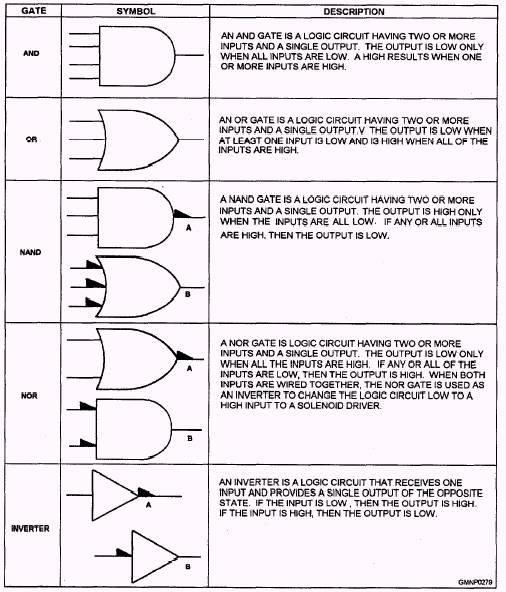
Logic Symbols The silicon chips in a logic circuit, called "gates," come in five varieties: AND, OR, NAND, NOR, and inverter. The most commonly used are the AND, OR, and inverter gates. Table 5-2 illustrates the symbol for Table 5-2.-Logic Circuit Symbology
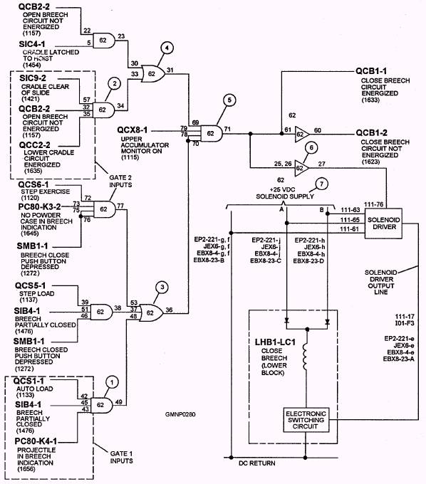
each gate and provides a brief description of its function. Logic Circuit Operation Figure 5-17 shows a typical logic circuit that uses inverted and buffered switch outputs to trigger a solenoid driver. The solenoid driver, in turn, controls a solenoid that initiates a gun-loading cycle, in this case, closing the breech of a Mk 45 Mod 1 gun. This circuit consists of AND gates, OR gates, and an inverter. The numbers within the gates identify the printed circuit board in the EP2 panel on which the circuit is located. The numbers on the input and output lines of the gates identify the terminal pin that connects to that point. The circled numbers in figure 5-17 are
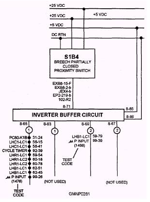
Figure 5-17.-Typical logic control circuit. added for ease in identifying items as we illustrate the operation of the circuit. Inputs to the logic gates are identified by both alphanumeric nomenclature and a brief description of what the input means. The input SIB4-1 (BREECH PARTIALLY CLOSED) to gate 1 comes from the number 1 output leg of the inverter buffer associated with SIB4 (fig. 5-18). When the breech is partially closed, the switch is activated and the high switch output through the inverter buffer produces a low logic input at input pin 45 of gate 1. Remember, gate 1 is an AND gate and requires all inputs to be LOW to produce a LOW output. The inputs to gates 1 and 2 in figure 5-17 initiate the operation of breech closing solenoid LHB1-LC1 in the normal mode of operation, AUTO LOAD. The six inputs indicate that the gun-loading system has delivered a complete round into the breech of the gun, the LOWER CRADLE circuit is energized, and the cradle has moved clear of the slide. With these conditions met, gates 1 and 2 pass a LOW logic signal to gates 3 and 4, respectively. Since gates 3 and 4 are OR gates, they require only one LOW input to produce a LOW output. The two LOWS from gates 3 and 4 are applied, with another LOW from summary circuit
Figure 5-18.-Inverter buffer circuit for SIB4. QCX8, to gate 5. When all inputs to gate 5 are LOW, it passes a LOW to gate 6, which is an inverter. With a LOW input, the inverter passes a HIGH output to the solenoid driver. This solenoid driver does not control the current flow to the solenoid. The output of the solenoid driver is used to forward bias a transistor circuit located in the solenoid housing. This output energizes the solenoid by allowing current to flow through the coil to DC RETURN. The A and B legs of the +25 VDC solenoid supply, point 7, represent a primary and secondary power supply to the solenoid. |
 |
|
|
||